
Accurate trace width calculations are essential for reliable high-current Pcb Design
When designing Power Electronics, motor controllers, or any application with currents above 1 ampere, guessing trace widths isnt an option. A trace thats too narrow will overheat, cause voltage drop, and potentially fail catastrophically. A trace thats too wide wastes valuable board space and increases manufacturing costs.
A Pcb Trace Width Calculator eliminates the guesswork by using established standards and physics-based formulas to determine the minimum trace width for your specific requirements. Whether your designing a 5A LED driver or a 50A battery management system, getting the trace dimensions right is crucial for reliability.
In this comprehensive guide, we'll explain the underlying principles, walk through the Ipc-2221 calculation method, and provide practical examples that show you exactly how to use trace width calculators effectively.
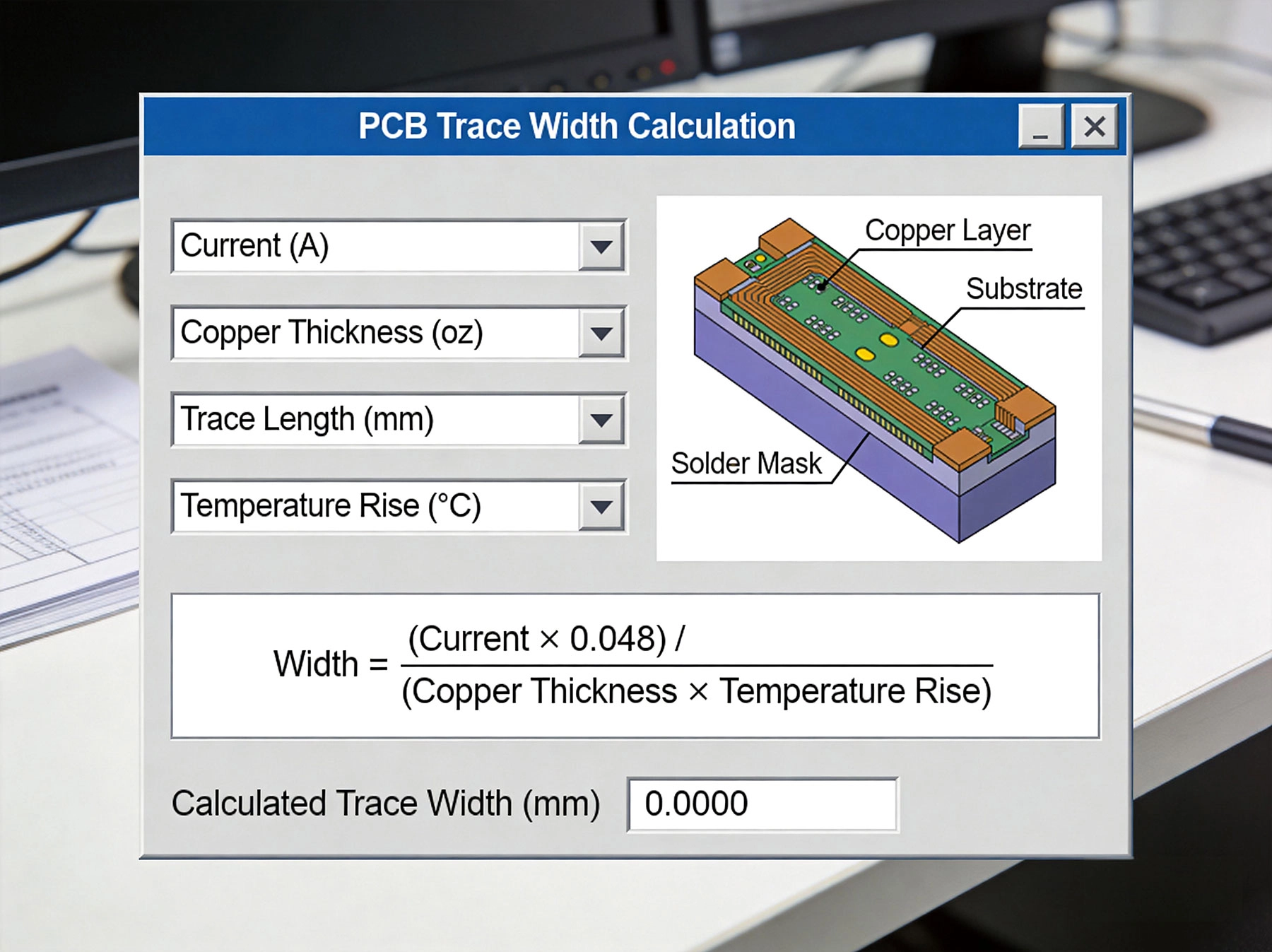
The Ipc-2221 Standard, published by the Association Connecting Electronics Industries, provides the most widely accepted formulas for calculating PCB Trace Current Capacity. This standard has been refined over decades and represents the collective experience of thousands of designers and manufacturers.
The formula for calculating current capacity based on trace cross-section is:
External Traces (on outer layers):
I = k × (ΔT)^0.44 × A^0.725
Internal Traces (buried within the PCB):
I = k × (ΔT)^0.44 × A^0.725 (with different k values)
Where:
This formula works by correlating the trace's cross-sectional area with its ability to dissipate heat. Larger traces can carry more current because they have more surface area for Heat Dissipation and lower electrical resistance.
External traces have better thermal dissipation because theyre exposed to air and can transfer heat through convection. Internal traces are surrounded by PCB substrate material (typically FR-4), which is a poor thermal conductor. Thats why internal traces require about 50% more width to carry the same current as external traces.
In practical terms, if your calculator gives you 200 mils for an external trace carrying 15A, plan for approximately 300 mils if that same trace runs on an internal layer.
This is your starting point - the maximum continuous current the trace needs to carry. Always consider the worst-case scenario, including surge currents. If your motor driver normally draws 8A but can spike to 12A during startup, design for 12A or higher.
A common mistake is designing for average current instead of peak current. Power supplies, motor drivers, and battery chargers often have significant current variations. Your trace must handle the peaks without overheating.
This parameter defines how much the trace temperature can increase above ambient. The IPC standard provides data for 10°C, 20°C, and 45°C temperature rises. Choosing the right value depends on your application:
Remember that a 20°C rise on a board operating in a 60°C environment means your trace reaches 80°C. Check the temperature ratings of nearby components to ensure compatability.
Copper Weight specifies the thickness of the copper layer, traditionally expressed in ounces per square foot:
Increasing Copper Weight reduces required trace width but also affects minimum trace/space capabilities and Manufacturing Cost. A 2 oz board typically costs 20-40% more than a 1 oz board.
While the IPC formula focuses on thermal considerations, voltage drop is equally important for many applications. The resistance of a trace causes voltage drop according to Ohm's law: V = I × R.
For a 1 oz copper trace, the resistance is approximately 0.5 milliohms per square. This means a 100 mil wide, 10 inch long trace has about 50 milliohms of resistance. At 10A, thats a 0.5V drop - significant in low-voltage applications.
Most advanced calculators include voltage drop calculations alongside thermal limits. If yours doesn't, calculate it separately using:
R = ρ × L / (W × T)
Where ρ is copper resistivity (1.7 × 10^-8 Ω·m at 20°C), L is length, W is width, and T is thickness.
Lets work through a practical example to illustrate the process. Suppose your designing a 12V battery charger that needs to carry 15A continuously.
Using an Ipc-2221 compliant calculator, enter:
The calculator returns approximately 185 mils (4.7mm) minimum trace width. This is your starting point, not your final answer.
For production designs, we recomend adding at least 30% margin:
185 mils × 1.3 = 240 mils (6.1mm)
This margin accounts for manufacturing variations, environmental factors, and long-term degradation. Its much cheaper to add extra copper during design than to redesign after field failures.
If your trace is 6 inches long:
This is acceptable for a 12V system (0.4% drop). For lower voltage systems like 3.3V or 5V, even small drops become critical.
A DC motor driver might have an average current of 5A but draw 15A during startup or stall conditions. If you calculate trace width based on 5A, the trace will overheat during peak loads. Always design for the worst-case current.
IPC values are based on specific conditions. If your PCB operates at high altitude, in vacuum, or at elevated temperatures, you need to derate the current capacity. Consult IPC-2221B Appendix for derating factors, or add extra margin.
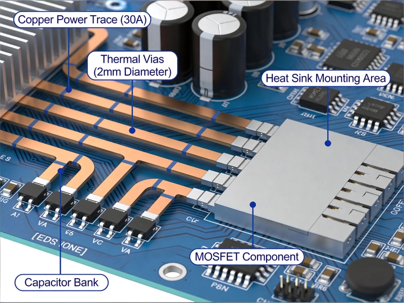
A 300 mil trace suddenly necking down to a single via creates a bottleneck. Vias have their own current limits - typically 1-3A depending on size and plating. When transitioning between layers, use multiple vias in parallel. A good rule of thumb: one via per 2A of current.
Many designers stick with 1 oz copper because its the default, then end up with impractically wide traces. For power applications, specify 2 oz or heavier copper. The Manufacturing Cost increase is justified by the space savings and thermal benefits.
A trace designed for 20°C temperature rise assumes it operates in isolation. If there are other heat-generating components nearby - power MOSFETs, inductors, or other high-current traces - the actual temperature rise will be higher. Use thermal simulation for complex layouts.
Advanced calculators automatically compute voltage drop based on trace dimensions and current. This is essential for low-voltage applications where even 100mV drop can be problematic.
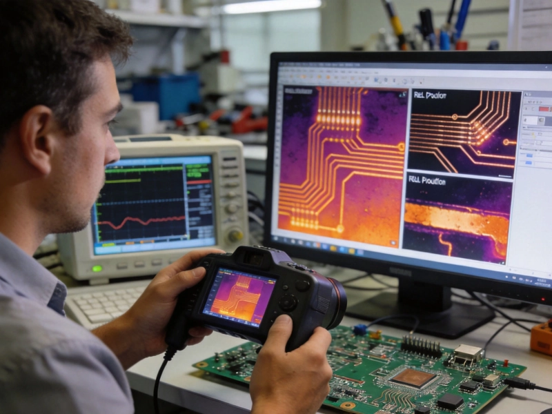
Some calculators link to Thermal Analysis tools that show the actual temperature distribution across your PCB. This helps identify hot spots that simple width calculations miss.
For boards with multiple copper layers, advanced calculators can compute total current capacity when traces are paralleled across layers with vias.
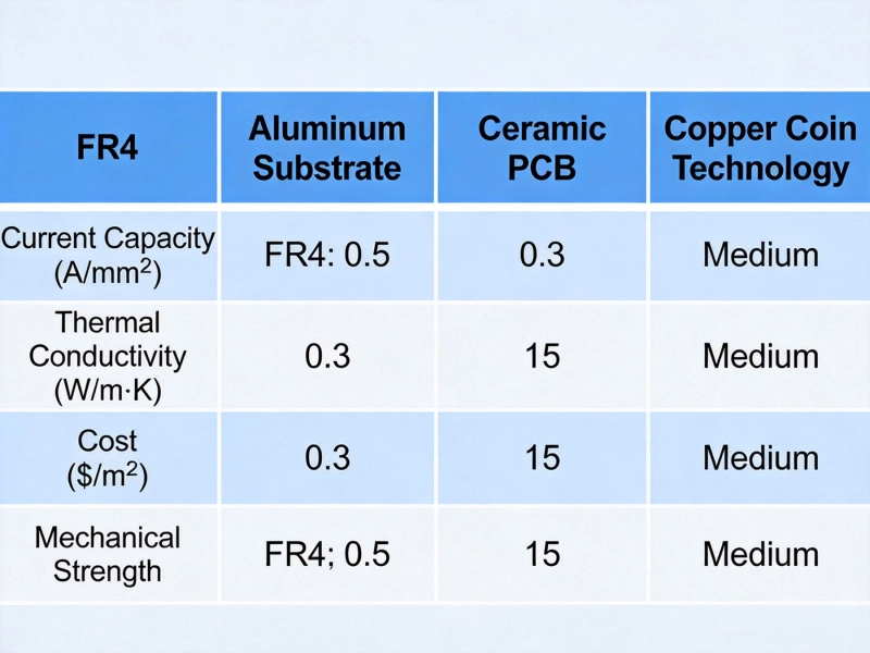
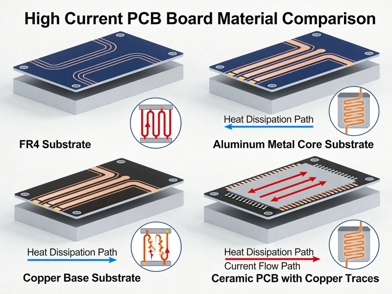
Standard calculators assume FR-4 substrate. If your using alternative materials like aluminum-core PCBs or ceramic substrates, look for calculators that allow thermal conductivity adjustments.
Professional calculators can import design files and automatically check all traces against current requirements. They can also export reports for design documentation.
Requirements: 5A continuous, 1 oz copper, external trace, 10°C rise
Calculator Result: 65 mils minimum
Recommended Width: 85 mils (with margin)
Notes: LED drivers are often in enclosed fixtures with limited cooling. Consider 20°C rise calculations if Thermal Management is limited.
Requirements: 25A peak, 2 oz copper, external trace, 20°C rise
Calculator Result: 250 mils minimum
Recommended Width: 325 mils (with margin)
Notes: Add copper pours around the motor driver IC. Use Thermal Vias to inner ground planes for Heat Dissipation.
Requirements: 40A continuous, 3 oz copper, external trace, 10°C rise
Calculator Result: 280 mils minimum
Recommended Width: 365 mils (with margin)
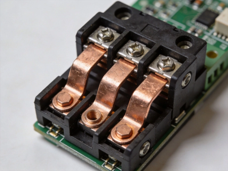
Notes: For currents above 30A, consider using copper pours instead of individual traces. Also evaluate bus bars or terminal blocks for connections.
Requirements: 20A continuous, 1 oz internal copper, 20°C rise
Calculator Result: 400 mils minimum
Recommended Width: 520 mils (with margin)
Notes: Internal traces have poor thermal dissipation. Where possible, route high currents on external layers and use Thermal Vias for layer transitions.
Calculated trace widths assume perfect manufacturing. In reality, etching tolerances mean your 200 mil trace might actually be 195-205 mils. For critical applications, verify with your PCB manufacturer what tolerances they guarantee.
Conformal coating reduces thermal dissipation from external traces. If your board will be coated, increase trace width by 10-20% or use more conservative temperature rise values.
Traces that heat and cool repeatedly experience thermal stress. Over time, this can cause via failures, delamination, or solder joint cracks. Design with margin to minimize temperature cycling amplitude.
Current doesn't distribute evenly through a trace - it concentrates at edges and corners (the "skin effect" at high frequencies). For very high frequency or fast-rise-time currents, the effective current-carrying area is reduced. Consult Ipc-2152 for high-frequency derating.
A Pcb Trace Width Calculator is an essential tool for any Power Electronics Design. By understanding the underlying IPC-2221 formulas and the parameters that affect current capacity, you can make informed decisions that balance electrical requirements, thermal management, and board space constraints.
Key takeaways:
With proper calculation and good design practices, your high-current Pcb Traces will deliver reliable performance throughout your product's lifetime.
The most accurate calculators implement the Ipc-2221 Standard and allow you to specify all relevant parameters. Saturn PCB Toolkit is widely used by professionals. Online calculators from reputable PCB manufacturers (4PCB, Advanced Circuits) are also reliable for most applications.
For pulsed currents, you need to consider the duty cycle and pulse duration. Short pulses can be carried by narrower traces because the thermal mass absorbs the energy. Use thermal simulation or consult IPC-2221B for pulsed current derating factors.
Standard calculators are designed for rigid PCBs. Flexible PCBs have different thermal characteristics and copper adhesion properties. Consult your flex PCB manufacturer for appropriate derating factors - typically 20-30% additional width is recommended.
For most applications, 10-20°C temperature rise is appropriate. Use 10°C for high-reliability applications, 20°C for standard consumer/industrial products, and 45°C only when space is extremely limited and thermal management has been thoroughly analyzed.
Online calculators based on IPC-2221 are accurate for their stated assumptions. However, they don't account for your specific thermal environment, nearby heat sources, or manufacturing variations. Use them as a starting point and add appropriate margins for production designs.
How to Design High Current PCB Traces: A Complete GuideMay/20/2026

High Current PCB Design Guidelines: Ensuring Reliability and SafetyJune/08/2026
Best Material for High Current PCB DesignMay/21/2026
High Current PCB Connector Selection: Test Results and Real Performance DataMay/21/2026
High Current PCB Connector Selection Guide: Choosing the Right Power Connectors for Your Electronics ProjectsJune/12/2026
Best Material for High Current PCB Design: How to Choose the Right SubstrateJune/05/2026
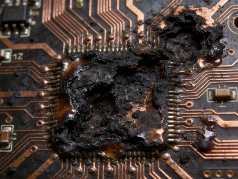
High Current PCB Failure Modes and PreventionJune/18/2026
Copper Pour vs Trace: What 3 Years of PCB Failures Taught UsMay/21/2026