
Understanding PCB Trace Current Capacity is essential for designing reliable power circuits
Every electronics engineer eventually asks: how much current can this Pcb Trace actually handle? It's not an academic question - get it wrong, and your board might overheat, fail prematurely, or even create a fire hazard. Get it too conservative, and you waste valuable board real estate on oversized traces. The answer depends on multiple factors that must be carefully analyzed during design.
Current flowing through a copper trace generates heat due to electrical resistance. The trace must dissipate this heat through conduction to the PCB substrate, convection to surrounding air, and radiation. If heat generation exceeds dissipation, temperature rises continuously until either equilibrium is reached or failure occurs. Designing reliable PCBs means ensuring equilibrium occurs at acceptable temperatures.
In this comprehensive guide, we'll explore the physics, standards, calculations, and practical considerations that determine PCB Trace Current Capacity. Whether your designing a low-power sensor board or a high-current motor controller, this knowledge is essential for creating reliable, long-lasting electronics.
Every conductor has resistance, and copper traces are no exception. The resistance of a Pcb Trace depends on its dimensions and copper resistivity:
R = ρ × L / (W × T)
Where:
Current flowing through this resistance generates power dissipation:
P = I² × R
Where I is current in amperes. This power manifests as heat, raising the trace temperature.
Copper's resistance isn't constant - it increases with temperature by approximately 0.4% per degree Celsius. This creates a potential thermal runaway condition:
Proper trace design breaks this cycle by ensuring Heat Dissipation matches or exceeds heat generation at a stable temperature point.
Heat escapes from a PCB trace through three primary paths:
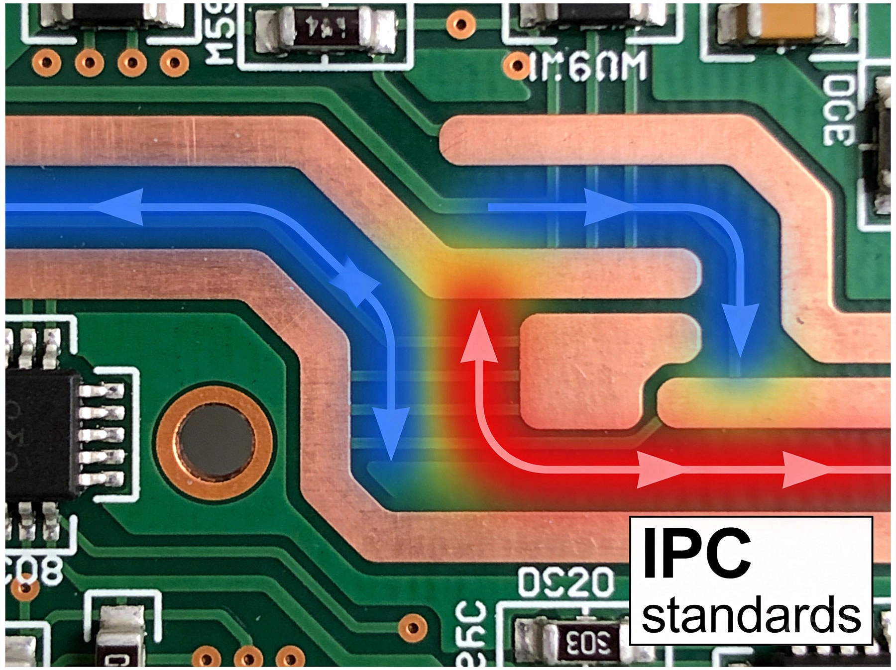
This explains why external traces handle more current than internal traces - they benefit from convection directly to air, while internal traces rely only on conduction through the substrate.
The Ipc-2221 Standard, published by the Association Connecting Electronics Industries, provides the most widely accepted method for calculating PCB trace current capacity. This standard represents decades of empirical testing and industry experience, making it the foundation for trace width calculators worldwide.
The standard correlates trace cross-sectional area with current capacity for various temperature rises. The empirical relationship follows this formula:
I = k × (ΔT)^0.44 × A^0.725
Where:
This formula works because Heat Dissipation is roughly proportional to surface area, which scales linearly with trace dimensions, while heat generation is related to cross-sectional area. The exponents reflect these physical relationships.
Ipc-2221 provides data for three standard temperature rise values:
| Temperature Rise | Application Type | Notes |
|---|---|---|
| 10°C | High-reliability applications | Medical devices, automotive, military. Traces stay cool, maximizing lifespan. |
| 20°C | Standard industrial/consumer | Most common choice. Balances reliability with space efficiency. |
| 45°C | Space-constrained designs | Use cautiously. Higher temperatures stress components and solder joints. |
Remember: temperature rise is the increase above ambient. A 20°C rise in a 50°C enclosure means the trace reaches 70°C.
The constant k differs significantly between external and internal traces:
This means internal traces need approximately 2× the cross-sectional area to carry the same current as external traces. The exact ratio varies with temperature rise but typically falls between 1.8:1 and 2.2:1.
Width is the most obvious factor - wider traces have lower resistance and larger surface area for heat dissipation. The relationship isn't linear due to thermal effects. Doubling trace width less than doubles current capacity because heat dissipation doesn't increase proportionally with width.
For a 1 oz external trace with 20°C temperature rise:
Copper Weight directly affects both resistance and thermal mass:
Heavier copper also increases thermal mass, providing a larger heat reservoir that slows temperature changes during transients.
Length affects resistance (longer = higher resistance) but doesn't directly affect thermal limits in Ipc-2221 calculations. However, longer traces have more total resistance, causing more voltage drop and potentially more total heat generation.
For a 1 oz, 100 mil wide trace:
In low-voltage systems, voltage drop often becomes the limiting factor before thermal limits.
External vs. internal layer placement dramatically affects current capacity:
When possible, route high-current traces on external layers. If internal routing is necessary, increase width by 40-60% and consider Thermal Vias to external copper.
Higher ambient temperatures reduce available temperature rise margin. A 20°C rise at 25°C ambient reaches 45°C, acceptable for most components. The same rise at 50°C ambient reaches 70°C, approaching limits for many capacitors and connectors.
For high-temperature environments, reduce the design temperature rise or specify higher temperature components.
Conformal coating reduces convection heat transfer from external traces. If your board will be coated, increase trace width by 10-20% or reduce design temperature rise accordingly.
Current capacity for external traces with 20°C temperature rise:
| Trace Width | Current Capacity | Typical Applications |
|---|---|---|
| 10 mils (0.25mm) | 1.0A | Low-power signal routing |
| 25 mils (0.64mm) | 1.8A | Moderate Power Distribution |
| 50 mils (1.27mm) | 2.8A | LED drivers, small motors |
| 100 mils (2.54mm) | 4.4A | Power supplies, medium motors |
| 200 mils (5.08mm) | 7.0A | Motor controllers, inverters |
| 400 mils (10.16mm) | 11A | High-power applications |
For internal traces, multiply these values by approximately 0.5.
Current capacity for external traces with 20°C temperature rise:
| Trace Width | Current Capacity | Typical Applications |
|---|---|---|
| 50 mils (1.27mm) | 6.0A | Power Distribution |
| 100 mils (2.54mm) | 9.5A | Motor drivers, chargers |
| 150 mils (3.81mm) | 12.5A | High-current power paths |
| 200 mils (5.08mm) | 15A | Industrial power supplies |
| 300 mils (7.62mm) | 20A | Very High Current applications |
Example 1: 5V/3A USB Charger
Example 2: 12V/10A LED Driver
Example 3: 24V/25A Motor Controller
Example 4: Internal Power Plane
While thermal limits determine the maximum current a trace can handle, voltage drop often becomes the practical limit, especially in low-voltage systems:
Vdrop = I × R
Where resistance depends on trace dimensions:
R = ρ × L / (W × T)
For 1 oz copper traces:
R ≈ 0.5 milliohms × (L / W)
Where L is length in inches and W is width in mils.
5V system with 3A load:
3.3V system with 2A load:
12V system with 20A load:
Voltage drop becomes critical in:
In these cases, you may need wider traces than thermal limits require, or consider using heavier copper or parallel traces.
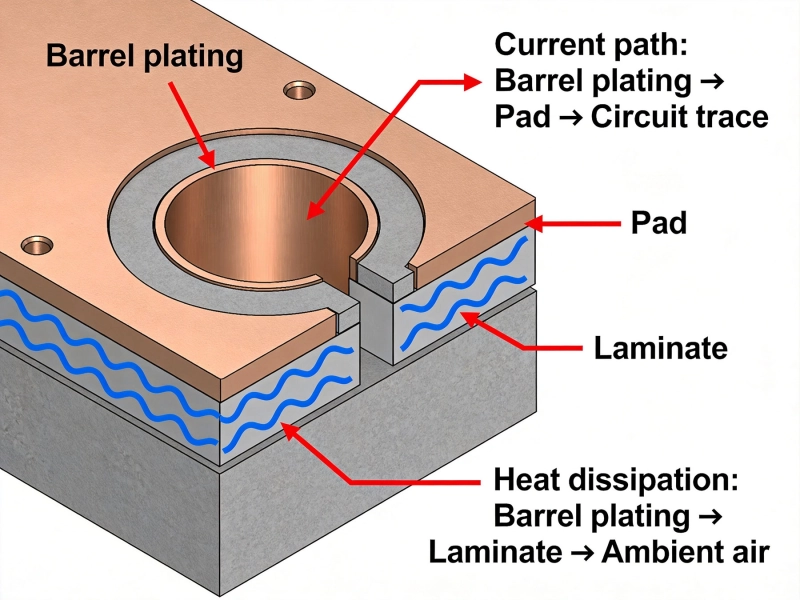
Vias are often overlooked but critical in high-current designs. A 300 mil trace suddenly necking down to a single via creates a bottleneck that becomes the limiting factor. Vias have their own current limitations due to their smaller cross-sectional area and limited heat dissipation.
Current capacity depends on via diameter, plating thickness, and temperature rise:
| Via Diameter | Plating | Current Capacity (10°C rise) |
|---|---|---|
| 0.3mm (12 mils) | 1 oz | 0.8-1.0A |
| 0.6mm (24 mils) | 1 oz | 1.8-2.2A |
| 0.8mm (32 mils) | 1 oz | 2.5-3.0A |
| 1.0mm (40 mils) | 2 oz | 4.0-5.0A |
For high-current transitions between layers:
When placing multiple vias:
A 20A current path might use 10-12 standard vias or 4-6 large-diameter vias. This seems excessive, but remember: each via carries only a fraction of the total current.
When board space prevents using a single wide trace, parallel traces can share current:
For very high currents, consider copper pours or planes instead of discrete traces:
At high frequencies (above ~100kHz), current concentrates near the conductor surface (skin effect). This reduces the effective cross-sectional area:
For pulsed or intermittent currents, thermal mass provides buffering:
Repeated temperature cycling causes mechanical stress:
This can cause delamination, via failures, or solder joint cracks
Calculated minimum values represent theoretical minimums under ideal conditions. Real-world factors include:
If a calculator gives you 150 mils minimum width:
Consider the cost of failure:
The cost of adding copper margin during design is trivial compared to these potential costs. A few extra mils of trace width costs almost nothing but can prevent catastrophic failures.
Several reliable calculators implement IPC-2221:
Many Pcb Design tools include built-in calculators or DRC rules:
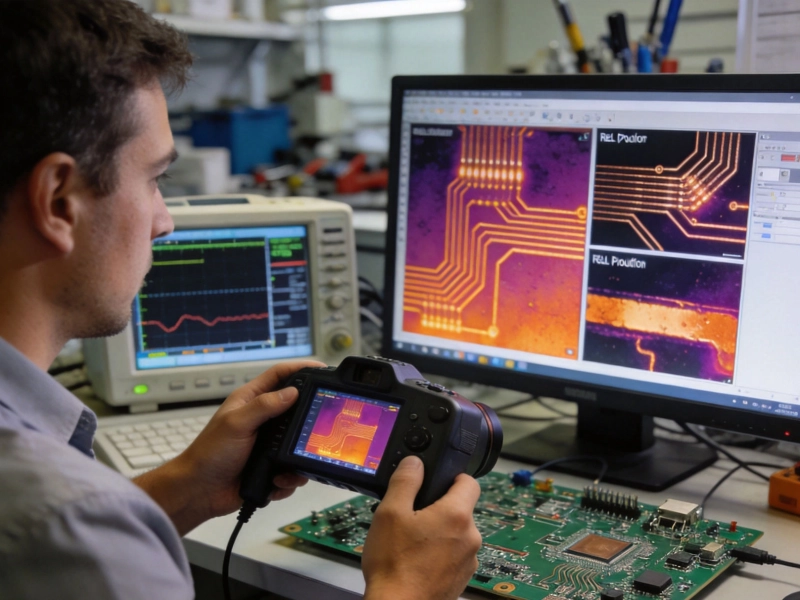
For critical applications, consider physical testing:
A common error is sizing traces for average instead of peak current. Motor drivers, power supplies, and inductive loads often have current spikes 2-3× average values. Always design for worst-case current including surges and fault conditions.
We've seen designs with wide traces necking down to a single via at a component pad. That via becomes a fuse. Always verify via capacity matches trace capacity, and use multiple vias for high-current transitions.
Thermal limits are important, but voltage drop often limits first in low-voltage systems. Always calculate both thermal and electrical limits. The higher one is your true limit.
Using the calculated minimum width is tempting to save space, but invites failure. Manufacturing variations, environmental factors, and unexpected conditions all stress designs beyond their theoretical minimums.
Many calculators default to 1 oz copper. If your board uses different copper weights, ensure the calculator accounts for it. Using wrong values leads to either oversized or undersized traces.
Internal traces need significantly more width than external traces. Forgetting this creates overheating issues on inner layers. Always specify trace location correctly in calculations.
A design that works at 25°C ambient may fail at 50°C ambient. Consider your operating environment: enclosed electronics, outdoor installations, or industrial settings all affect thermal performance.
Understanding how much current a PCB trace can carry is fundamental to designing reliable electronics. The answer depends on multiple interrelated factors: trace dimensions, copper thickness, layer location, ambient temperature, and acceptable temperature rise. The Ipc-2221 Standard provides a proven methodology for calculating current capacity based on empirical data.
Key principles to remember:
Whether your designing a low-power sensor board or a high-current industrial power supply, proper trace sizing ensures reliable, long-lasting performance. The investment in proper current capacity calculations pays dividends in reduced field failures, improved product reputation, and lower total cost of ownership.
There's no absolute maximum - it depends on trace dimensions, copper thickness, and acceptable temperature rise. Practical limits range from a few amps for narrow signal traces to 50+ amps for very wide traces on heavy copper boards. Use IPC-2221 calculators to determine capacity for your specific requirements.
Use the IPC-2221 formula: I = k × (ΔT)^0.44 × A^0.725, where k = 0.048 for external traces and 0.024 for internal traces, ΔT is temperature rise in °C, and A is cross-sectional area in square mils. Or use an online calculator that implements this standard.
A common rule of thumb: 1 oz copper external traces can carry approximately 1A per 20 mils of width with 20°C temperature rise. For example, 40 mils ≈ 2A, 80 mils ≈ 4A, 160 mils ≈ 8A. This is approximate - always use proper calculations for production designs.
Yes, 20A is achievable with proper design. On 1 oz copper, you'd need approximately 300 mils (7.6mm) wide external traces. On 3 oz copper, this reduces to about 140 mils (3.6mm). Ensure via transitions use multiple vias in parallel and add appropriate design margins.
A standard 0.3mm via with 1 oz plating handles approximately 0.8-1.0A. Larger vias carry more current. For high-current applications, use multiple vias in parallel - a common rule is one via per 2A of current.
Yes, internal traces need 40-60% more width than external traces to carry the same current. Internal traces can only dissipate heat through conduction into the PCB substrate, while external traces benefit from convection cooling to air.
Use 10°C temperature rise for high-reliability applications (medical, automotive, military). Use 20°C for standard consumer and industrial products. Use 45°C only when space is extremely limited and you've thoroughly analyzed thermal effects.
Recommended margins vary by application: 20% for hobby/prototype, 30-40% for consumer products, 40-50% for industrial/commercial, and 50-100% for safety-critical systems. Margins account for manufacturing variations and unexpected operating conditions.
Best Material for High Current PCB DesignMay/21/2026
Best Material for High Current PCB Design: How to Choose the Right SubstrateJune/05/2026
High Current PCB Connector Selection: Test Results and Real Performance DataMay/21/2026
Plated Through Hole Current Rating for PCBsJune/10/2026

High Current PCB Design Guidelines: Ensuring Reliability and SafetyJune/08/2026
Copper Pour vs Trace: What 3 Years of PCB Failures Taught UsMay/21/2026
High Current PCB Connector Selection Guide: Choosing the Right Power Connectors for Your Electronics ProjectsJune/12/2026

5 Critical Thermal Management Problems in High Power PCBsMay/21/2026