
Everything you need to design reliable power electronics—from trace widths to Thermal Management
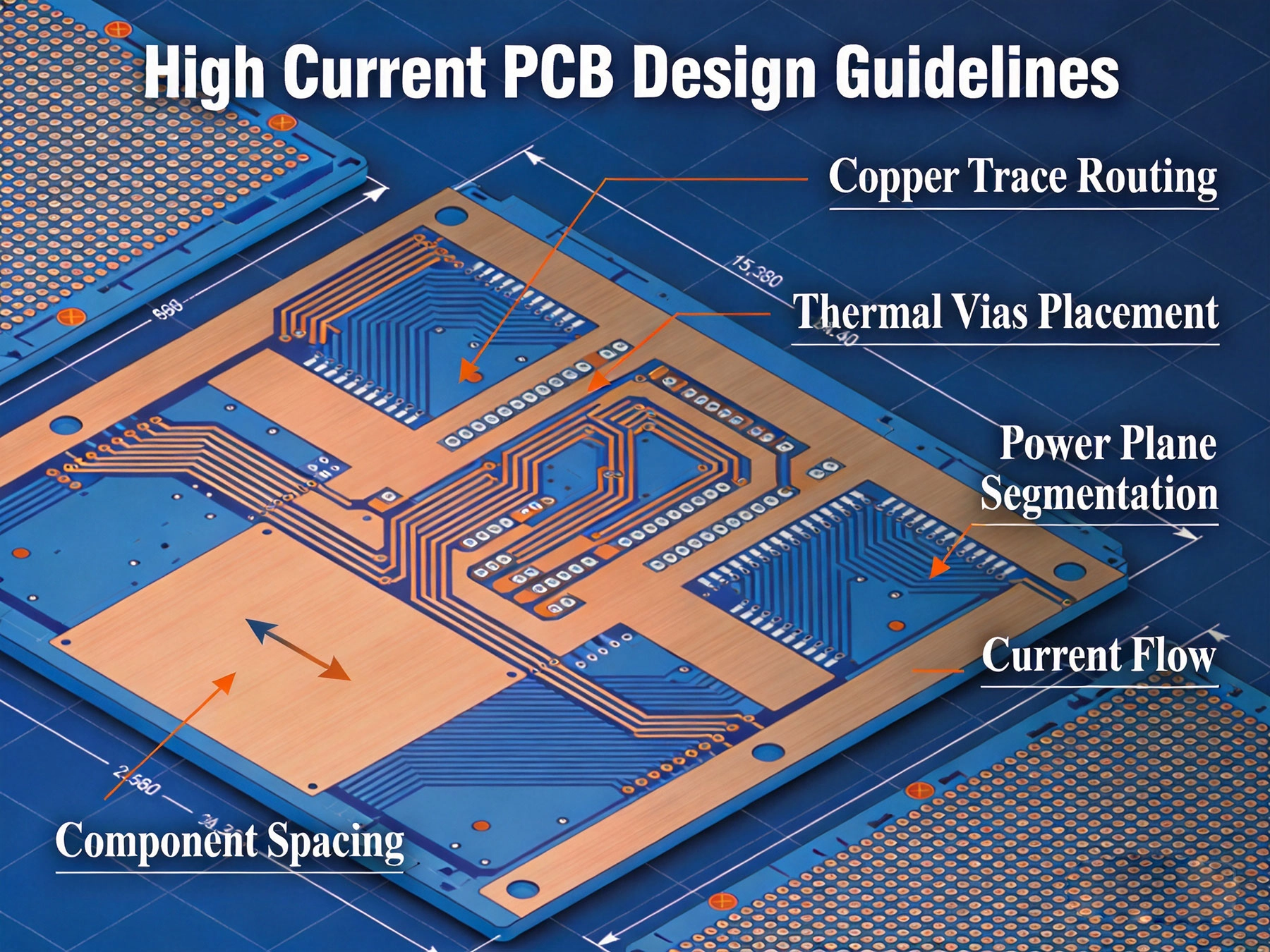
When current exceeds about 10A, your PCB design enters a different world. Below that threshold, standard practices work fine. Above it, you're fighting physics—resistive heating, voltage drop, electromagnetic interference, and Thermal Management become dominant concerns.
I've designed PCBs handling from 10A to 500A across applications from LED drivers to EV chargers. Here's what I've learned the hard way, consolidated into actionable guidelines you can use today.
A client once sent 500 motor control boards to manufacturing without proper thermal validation. After three weeks of field failures, they discovered the high-current traces were undersized by 40%. The root cause? Trusting an online calculator without understanding the assumptions. This guide will save you from that fate.
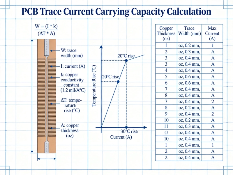
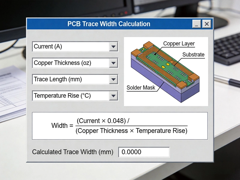
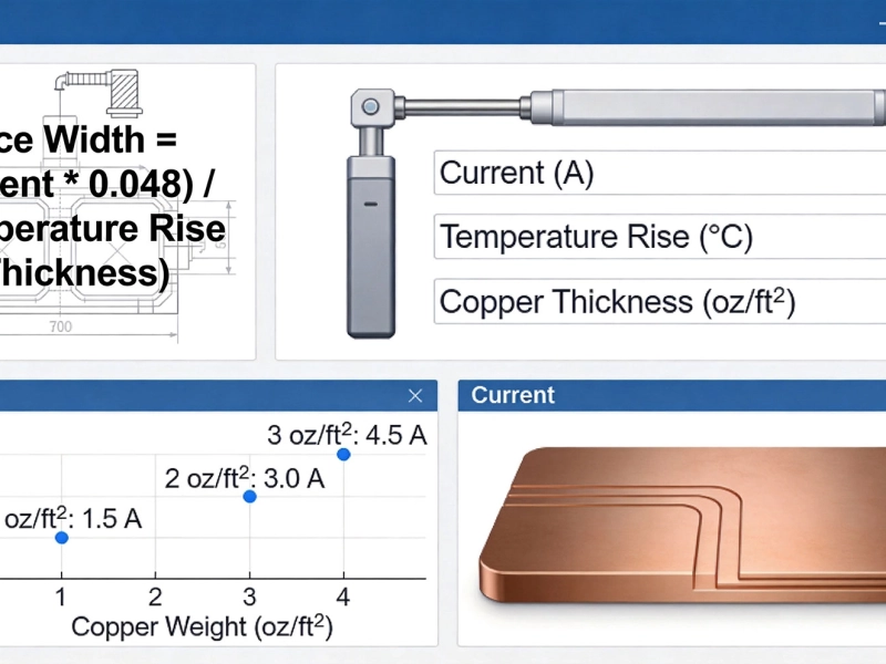
Forget IPC-2221 lookup charts—they're outdated and overly conservative. Ipc-2152 gives you physics-based calculations that account for your actual conditions:
| Parameter | Definition | Typical Values |
|---|---|---|
| I | Current (Amps) | Design requirement |
| k | Correction factor | 0.024 (external, still air) |
| ΔT | Temperature rise (°C) | 10°C (conservative) / 20°C (standard) |
| A | Cross-sectional area (sq mils) | Width × Thickness |
Always add 25% to calculated trace widths. Conditions in the field are never as good as your calculation assumes—ambient temperature varies, airflow gets blocked, and components age.
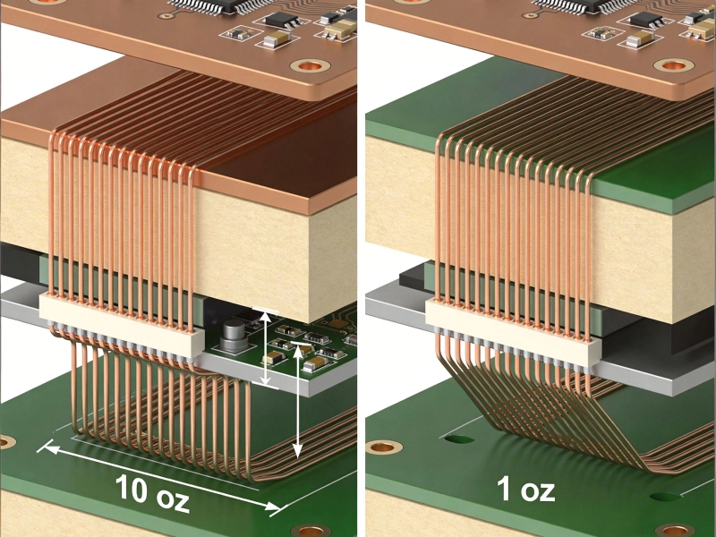
Copper weight dramatically affects your current capacity and thermal performance. Here's the practical breakdown:
| Copper Weight | Thickness | Best For | Current Capacity* |
|---|---|---|---|
| 1 oz (standard) | 0.7 mil / 18 μm | Signal traces, low power | To ~10A with wide traces |
| 2 oz | 1.4 mil / 35 μm | Power rails, moderate current | 10-30A practical range |
| 3 oz | 2.1 mil / 53 μm | High current paths | 20-50A with good layout |
| 4+ oz | 2.8+ mil / 70+ μm | Extreme current, busbars | 50A+ and specialized apps |
*Assuming 20°C rise, external traces, still air. Internal traces need approximately 2× the width.
Every PCB has four ways to shed heat. Understanding these helps you design effective cooling:
Thermal Vias transfer heat from hot components to internal copper planes or the board's bottom layer. They're essential for any component dissipating more than 1W.
Internal copper planes do double duty—they're your primary heat distribution network. Design them strategically:
For high current designs, divide your power distribution into zones based on current levels:
Ground currents flow through shared copper, creating voltage differences between sections. This causes noise coupling and measurement errors in high current systems.
All ground returns connect at a single point near the power input. Each high-current section has its own dedicated return path. This eliminates ground loop interference.
High current switching creates voltage transients. Size your decoupling strategically:
| Application | Capacitor Location | Recommended Values |
|---|---|---|
| Input bulk decoupling | Within 5mm of power input | 100μF + 10μF ceramic |
| Switching node bypass | Directly under MOSFET/IC pins | 1-10μF ceramic (X5R/X7R) |
| High-frequency decoupling | As close as possible to power pins | 100nF - 1μF ceramic |
| Output filtering | Near output connector | 10-100μF bulk + 1-10μF ceramic |
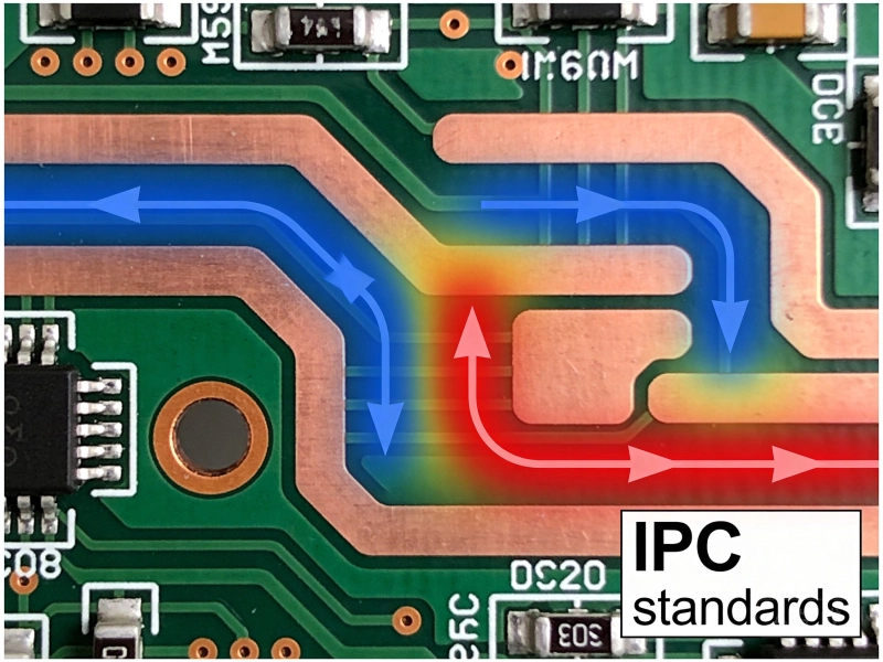
90° corners create current crowding and increase effective resistance. Use mitered 45° corners or rounded arcs instead. The difference? About 5-10% higher resistance at the bend.
Vias add resistance (about 0.5mΩ per plated through-hole). For currents above 10A, each via represents measurable voltage drop. If you must use vias, use multiple in parallel—6 vias will carry 3× the current of 2.
Sudden width changes cause current crowding at transitions. If you must change width (connecting to a component pad), transition gradually over 2-3mm, not abruptly.
Thermal reliefs help soldering but impede current flow and heat spreading. For high-current connections, use wider spokes (10-12 mil) or remove relief entirely on the thermal pad—solder the connection properly during assembly.
Adjacent high-current traces heat each other. If traces carry current in the same direction and are closer than 3× trace width, add 25-50% extra width to account for reduced cooling.
Hot components cook nearby components. Maintain minimum spacing based on thermal simulation, but generally keep temperature-sensitive parts (electrolytic caps, crystals) at least 20mm from power semiconductors.
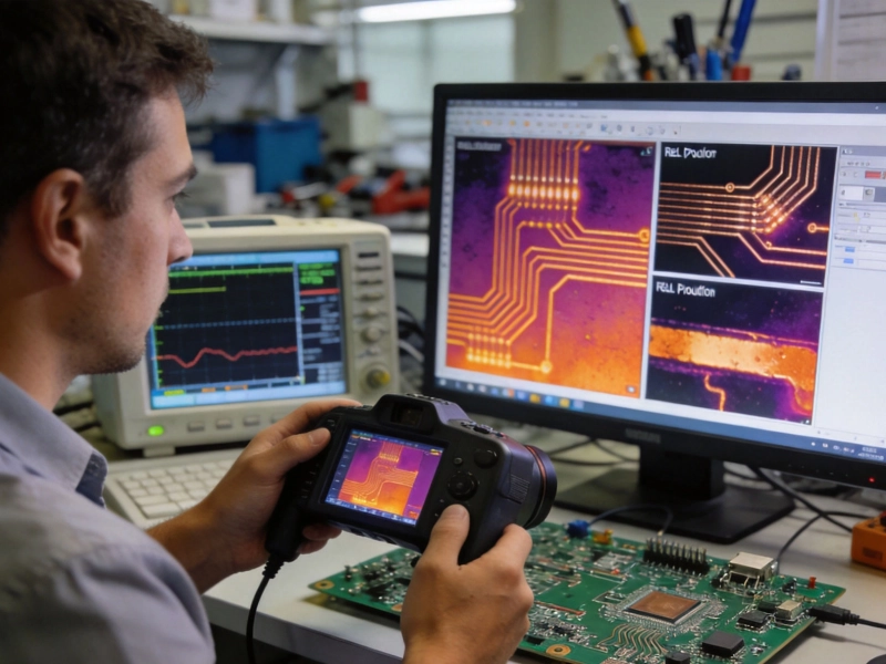
Building and testing is too late to find thermal problems. Run thermal simulation early (even free tools like KiCad's thermal analysis) and iterate before you commit to manufacturing.
| Condition | Minimum Spacing | Why It Matters |
|---|---|---|
| High voltage (>400V) | 0.5mm per 100V + safety margin | Creepage and clearance requirements |
| High current traces | 3× trace width between parallel runs | Thermal proximity effect |
| Thermal pad to nearby traces | 2mm minimum | Heat spreading without coupling |
| Electrolytic caps from power devices | 20mm minimum | Capacitor lifetime degradation |
| Input to output isolation | Per safety standard requirements | Reinforced isolation for AC inputs |
The thermal pad under a power semiconductor is often its primary heat escape route. Design it correctly:
Connector ratings assume ideal conditions. Derate them for real-world use:
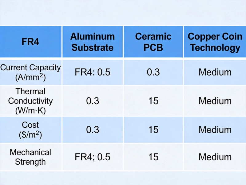
For extreme currents (>50A) or when you need localized low resistance, embed copper coins in your PCB:
When connectors can't handle your current, consider press-fit terminals that go through the entire board:
For currents above 100A, consider external busbars:
| Category | Key Requirements | Acceptable Range |
|---|---|---|
| Trace Width | Calculate per IPC-2152 | +25% safety margin minimum |
| Copper Weight | Match current requirements | 2-3 oz for most 10-50A designs |
| Thermal Vias | Under all power components | 6×6 grid, 0.3mm drill, 1mm pitch |
| Ground Design | Star topology for power circuits | Single point near power input |
| Component Spacing | Thermal and electrical separation | 20mm min for heat-sensitive parts |
| Validation | IR camera and thermocouple testing | No hotspots above 105°C |
These guidelines give you the foundation for reliable Power Electronics Design. Start with calculations, validate with simulation, and always test with thermal imaging before committing to production.
IPC-2152 Current Carrying Capacity: The Definitive PCB Trace Calculator GuideMay/21/2026
Heavy Copper vs Standard Copper PCB: Complete Comparison Guide for EngineersMay/20/2026
High Current PCB Trace Width Calculator: Complete Guide with Formulas and ExamplesMay/20/2026
Copper Pour vs Trace: What 3 Years of PCB Failures Taught UsMay/21/2026
Plated Through Hole Current Rating: Complete Guide for PCB DesignersMay/21/2026
High Current PCB Trace Width Calculator: The Ultimate Engineering GuideMay/20/2026
How Much Current Can a PCB Trace Carry? Complete Engineering GuideMay/20/2026
Best Material for High Current PCB DesignMay/21/2026