
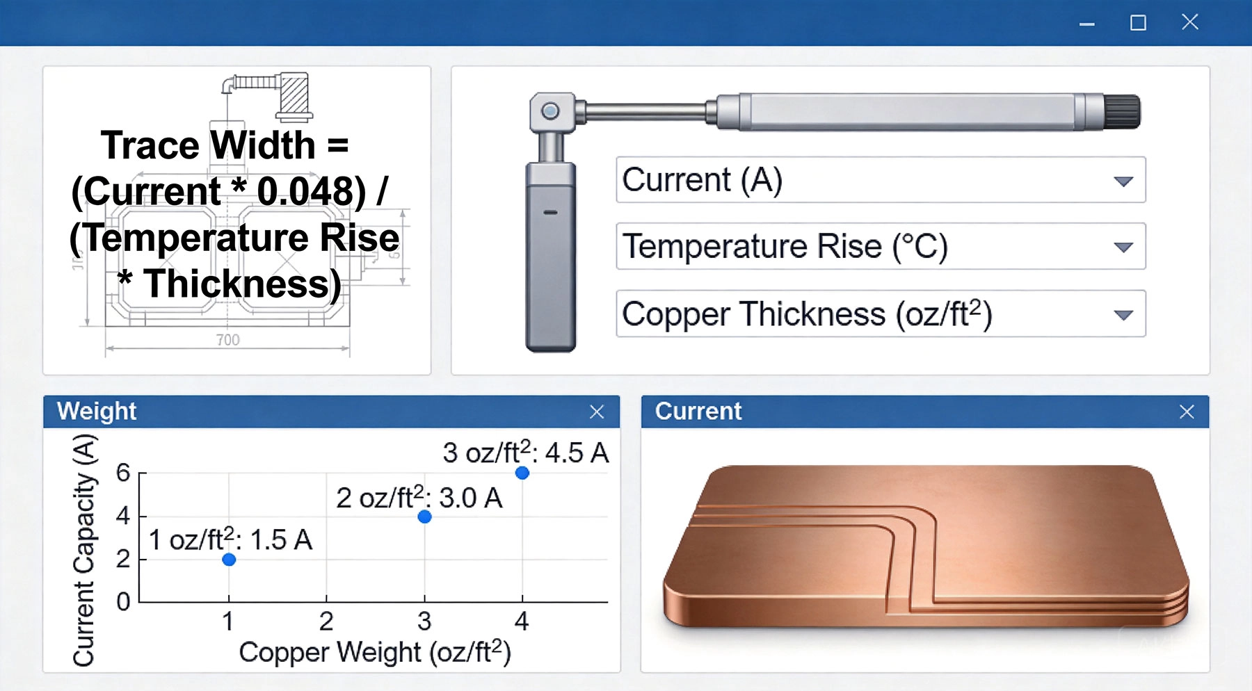
A trace width calculator helps engineers determine the right copper dimensions for safe Current Carrying Capacity
Every electronics engineer faces the same challenge when designing power circuits: how wide should the traces be to safely carry the required current? Get it wrong, and you risk board failure, component damage, or even fire hazards. Get it too conservative, and you waste precious board real estate. Thats where a High Current Pcb Trace Width Calculator becomes your most valuable design tool.
A trace width calculator uses established industry standards to determine the minimum copper width needed to carry a specific current without exceeding temperature limits. These calculators have evolved from simple lookup tables to sophisticated software tools that account for multiple variables including Copper Thickness, trace location, ambient temperature, and acceptable temperature rise.
In this guide, we'll dive deep into how these calculators work, the science behind them, and how to use them effectively for your Power Electronics designs. Whether your a hobbyist building your first motor controller or a professional engineer designing industrial power supplies, this information will help you make better design decisions.
Current flowing through a conductor generates heat proportional to the resistance and the square of the current (P = I²R). A Pcb Trace is essentially a flat copper resistor. The narrower the trace, the higher its resistance, and the more heat it generates for a given current. The calculator helps you find the balance point where heat generation equals Heat Dissipation at an acceptable temperature.
Copper's resistance increases with temperature - approximately 0.4% per degree Celsius. This creates a potential feedback loop: as the trace heats up, its resistance increases, causing more heat generation. Proper trace width design prevents this from becoming a runaway condition.
Heat escapes from a Pcb Trace through three primary paths:
This explains why internal traces need to be wider than external traces - they can only dissipate heat through conduction into the substrate, not through direct convection to air.
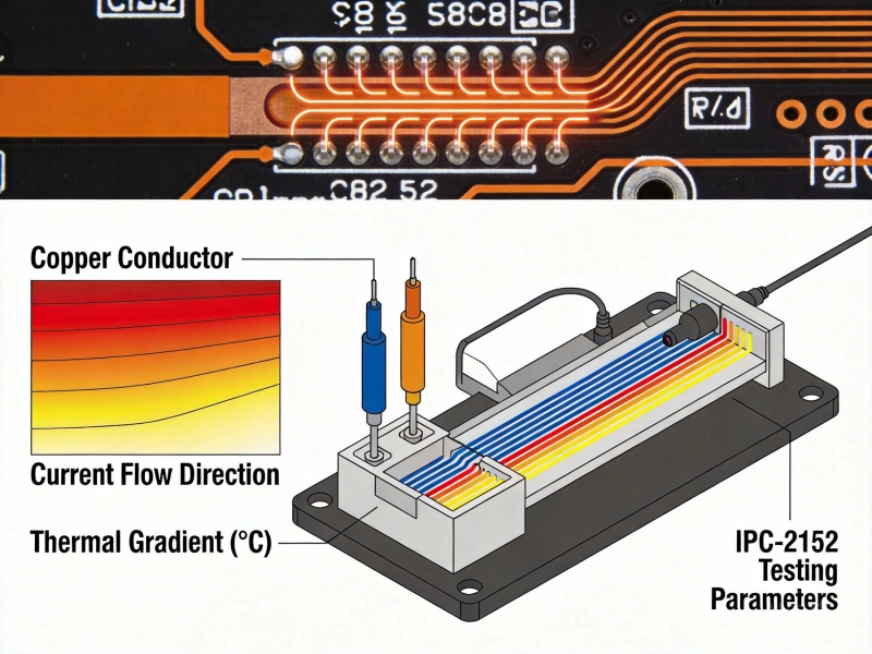
The Ipc-2221 Standard represents decades of empirical testing and serves as the foundation for most trace width calculators. The standard provides curves and formulas that correlate trace cross-sectional area with Current Carrying Capacity for various temperature rises.
The governing equation rearranged to solve for cross-sectional area is:
A = (I / (k × ΔT^0.44))^(1/0.725)
Where the constant k equals 0.048 for external traces and 0.024 for internal traces. From the cross-sectional area, you can calculate the required width by dividing by Copper Thickness.
This is the maximum continuous current the trace must carry. The critical question is: what current value should you enter? Consider these scenarios:
Steady-state DC applications: Use the maximum operating current. A battery charger delivering 10A continuously needs traces sized for 10A.
Motor drivers and inductive loads: Use the peak current, not the average. A motor drawing 5A average might draw 15A during startup. Design for the peak.
Pulsed loads: For short pulses, thermal mass provides some buffering. If duty cycle is low and pulses are brief, you can use an RMS current value. Consult IPC-2221B for detailed pulsed current guidelines.
This parameter defines how hot the trace gets compared to ambient temperature. Standard options are 10°C, 20°C, and 45°C. Heres how to choose:
10°C rise: Best for high-reliability applications, medical devices, automotive electronics, and situations with limited cooling. Traces stay cool and last longer.
20°C rise: The sweet spot for most consumer and industrial electronics. Balances reliability with space efficiency.
45°C rise: Use cautiously. Suitable only when space constraints are severe and you've thoroughly analyzed the thermal environment.
Remember: a 20°C rise means the trace reaches ambient + 20°C. In a 50°C industrial enclosure, that trace hits 70°C - check nearby component temperature limits.
Copper Weight, expressed in ounces per square foot, determines trace thickness:
| Copper Weight | Thickness | Typical Applications |
|---|---|---|
| 0.5 oz | 17.5 μm (0.7 mils) | High-density signal layers |
| 1 oz | 35 μm (1.4 mils) | Standard PCBs, default for calculators |
| 2 oz | 70 μm (2.8 mils) | Power Electronics, motor drivers |
| 3 oz | 105 μm (4.2 mils) | High-power supplies, battery systems |
| 4+ oz | 140+ μm (5.6+ mils) | Extreme power, Bus Bar replacements |
Heavier copper allows narrower traces but increases cost and minimum feature sizes. A 2 oz board costs roughly 30% more than 1 oz but may reduce required trace width by half.
External traces on outer PCB layers dissipate heat directly to air. Internal traces are buried in the substrate material (typically FR-4), which has poor thermal conductivity (about 0.3 W/m·K compared to copper's 400 W/m·K).
This means internal traces typically need 40-60% more width to carry the same current as external traces. When using a calculator, always specify the correct trace location.
Lets work through a complete design scenario to demonstrate the calculator in action.
Your designing a PCB for a 24V DC motor driver. The motor draws 12A at full load and can spike to 18A during startup. The board will be in an industrial enclosure with ambient temperature up to 45°C.
Using the Ipc-2221 formula for external traces:
I = 18A, ΔT = 20°C, k = 0.048
A = (18 / (0.048 × 20^0.44))^(1/0.725)
A ≈ 280 square mils
Width = A / thickness = 280 / 2.8 ≈ 100 mils (2.54mm)
For production reliability, add 40% margin:
Final width = 100 × 1.4 = 140 mils (3.56mm)
If the power trace runs 4 inches from connector to motor driver:
Resistance = (ρ × L) / (W × T)
R = (1.7×10^-8 × 0.1m) / (0.00356m × 70×10^-6m) ≈ 6.8 milliohms
Voltage drop at 18A = 18 × 0.0068 = 122mV
At 24V, this represents 0.5% loss - acceptable for this application.
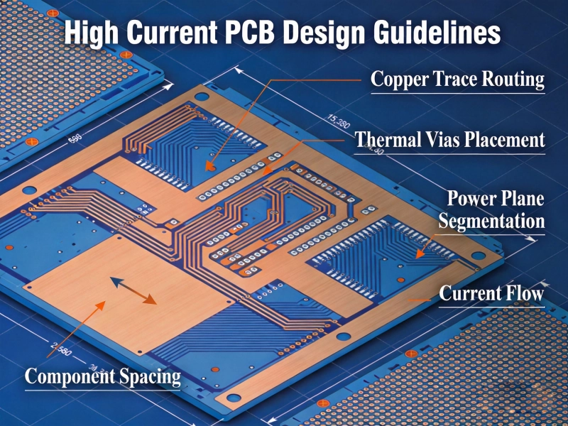
With the width determined, route the trace using these guidelines:
Sophisticated calculators show voltage drop alongside thermal limits. For low-voltage systems (3.3V, 5V), even small drops cause significant percentage losses. A 100mV drop on a 3.3V rail is 3% - potentially causing logic errors or brownout resets.
Some calculators let you specify maximum acceptable voltage drop and calculate the minimum width to meet both thermal and electrical requirements.
When board space prevents using a single wide trace, parallel traces can share the current. Advanced calculators compute total current capacity for multiple traces with specified spacing. Generally, traces spaced at least 3× their width apart share current effectively.
Vias are often the weak link in high-current paths. A standard 0.3mm via with 1 oz plating handles about 1A. Look for calculators that include via sizing or use this rule of thumb: provide one via per 2A of current, or use larger vias (0.6mm+) for higher currents per via.
Professional-grade calculators may link to thermal simulation software. These tools model the actual temperature distribution across your PCB, revealing hot spots that simple width calculations miss. For complex boards with multiple heat sources, thermal simulation is invaluable.
Many designers calculate trace width based on average current draw. But power supplies, motors, and inductive loads often have current spikes far above average. A trace sized for 5A average will fail when the motor stalls and draws 15A. Always design for maximum current.
We've seen designs with 200-mil traces necking down to a single 20-mil via at a component pad. That via becomes a fuse. Always verify your vias can handle the current, and use multiple vias in parallel for high-current connections.
The calculator assumes your trace operates in isolation. If it runs next to a hot MOSFET or under a warm inductor, the actual temperature rise will be higher. Either add extra margin or, better yet, relocate sensitive traces away from heat sources.
Room temperature is typically 25°C, but enclosed electronics can reach 50-70°C. If you designed for 20°C rise in a 25°C room, the trace reaches 45°C. In a 60°C enclosure, it reaches 80°C - potentially exceeding component limits.
The calculated width is the theoretical minimum. Manufacturing variations (etching tolerances, copper thickness variations) mean your actual trace might be 5-10% narrower. Environmental factors (altitude, humidity, airflow) affect thermal dissipation. Always add margin - we recomend 30-50% for production designs.
Application: USB power supply with 5V output at 3A
Parameters: 3A continuous, 1 oz copper, external trace, 10°C rise
Calculated width: 45 mils
Recommended width: 60 mils (with margin)
Design notes: Low voltage makes voltage drop critical. A 6-inch, 60-mil trace drops about 75mV - 1.5% of 5V. Keep traces short.
Application: LED driver powering multiple LED strips
Parameters: 20A continuous, 2 oz copper, external trace, 20°C rise
Calculated width: 200 mils
Recommended width: 280 mils (with margin)
Design notes: Consider Copper Pour instead of discrete trace. Add Thermal Vias to inner ground planes for additional Heat Dissipation.
Application: High-power EV onboard charger section
Parameters: 50A continuous, 3 oz copper, external trace, 20°C rise
Calculated width: 350 mils
Recommended width: 490 mils (with margin)
Design notes: At this current level, consider using copper pours across multiple layers connected with via arrays. Evaluate bus bars for terminal connections.
Application: Industrial controller with internal power plane
Parameters: 15A continuous, 1 oz internal copper, 20°C rise
Calculated width: 300 mils (internal traces need more width)
Recommended width: 420 mils (with margin)
Design notes: Use Thermal Vias every 0.5 inch to connect to outer layer copper for improved heat dissipation. Consider 2 oz copper on power layers.
While trace width calculators are incredibly useful, they have limitations:
High-frequency applications: Standard calculators don't account for skin effect, which reduces effective conductor area at high frequencies. For RF or fast-switching power electronics, consult specialized resources.
Extreme environments: Vacuum, high altitude, or exotic thermal environments require specialized analysis. The standard IPC values assume sea-level atmospheric pressure.
Transient analysis: Calculators give steady-state results. If your application has rapid current cycling, thermal transient analysis may be needed.
Complex thermal environments: Multiple heat sources, forced air cooling, or heatsinking arrangements affect trace temperatures in ways calculators can't model. Use thermal simulation software.
For critical applications - medical devices, automotive safety systems, aerospace - consider engaging Thermal Analysis specialists and conducting physical prototype testing.
A High Current Pcb Trace Width Calculator is an indispensable tool for Power Electronics Design. By understanding the underlying principles - thermal dissipation, the Ipc-2221 Standard, and the key parameters affecting current capacity - you can use these tools effectively and avoid common pitfalls.
Remember that the calculator gives you a starting point, not the final answer. Apply appropriate margins, consider your specific thermal environment, and verify with prototype testing. With careful design, your high-current Pcb Traces will provide reliable, long-lasting performance.
The investment in proper Trace Width Calculation pays dividends in reduced field failures, lower warranty costs, and improved product reputation. Whether your building a one-off prototype or designing for mass production, taking the time to calculate trace widths correctly is always worth the effort.
The best calculators implement Ipc-2221 standards and allow input of all key parameters. Saturn PCB Toolkit, DigiKey's online calculator, and Advanced Circuits' calculator are all reliable choices. For professional work, consider tools that integrate with your CAD software.
We recommend 30-50% margin for production designs. This accounts for manufacturing variations, environmental factors, and provides safety margin for unexpected conditions. For prototype or hobby projects, 20% minimum margin is acceptable.
Yes, parallel traces can effectively share current. Space them at least 3× trace width apart for optimal current sharing. Total current capacity is roughly the sum of individual trace capacities when properly spaced.
An undersized trace will overheat, potentially causing solder joint failure, delamination of the PCB substrate, or in extreme cases, open-circuit failure. It also causes voltage drop that may affect circuit performance. Always size traces appropriately.
External layers are preferred for high current due to better thermal dissipation. If you must use internal layers, increase width by 40-60% and use thermal vias to connect to outer layer copper for heat spreading.
IPC-2152 Current Carrying Capacity Calculation GuideJune/03/2026
Plated Through Hole Current Rating: Complete Guide for PCB DesignersMay/21/2026

Mastering IPC-2152 Current Carrying Capacity Calculation for Reliable PCB DesignJune/04/2026

High Current PCB Design Guidelines: Ensuring Reliability and SafetyJune/08/2026
Why Your High-Power PCBs Overheat (And the 5 Methods That Actually Fix It)May/20/2026
High Current PCB Design GuidelinesMay/21/2026

5 Critical Thermal Management Problems in High Power PCBsMay/21/2026
Best Material for High Current PCB DesignMay/21/2026