
Properly designed High Current Pcb traces ensure reliable power delivery in demanding applications
When your designing PCBs for Power Electronics, motor drivers, or high-current applications, the traces become critical components rather then just conductive paths. Unlike signal traces, High Current traces must handle significant power without overheating, maintain voltage integrity, and survive thermal cycling over the product's lifetime.
The stakes are high: undersized traces can cause voltage drops, excessive heat generation, and even catastrophic board failure. A trace that carries 10A might need to be 10x wider then a trace carrying 1A, and the design considerations go far beyond simple width calculations.
In this guide, we'll cover the essential principles and practical calculations you need to design reliable High Current Pcb traces, drawing from real-world experience in Power Electronics Design.
The most obvious factor is the cross-sectional area of the trace, determined by its width and Copper Thickness. Standard PCB Copper Thickness is 1 oz/ft² (approximately 35μm or 1.4 mils), but for High Current applications, designers often use 2 oz or even 3 oz copper. Heres the catch - increasing Copper Weight affects your minimum trace/space capabilities and increases cost.
The relationship between trace width and current capacity isn't linear. According to Ipc-2221 standards, a 10 mil wide trace with 1 oz copper can handle about 0.5A with 10°C temperature rise, but doubling the width doesn't double the current capacity due to thermal dissipation characteristics.
Every trace has a maximum allowable temperature rise above ambient. The standard Ipc-2221 provides tables for temperature rises of 10°C, 20°C, and 45°C. But in practice, you should consider your application's thermal environment. If your PCB will operate in a 70°C enclosure, a 20°C temperature rise means your trace reaches 90°C - thats getting close to many component temperature limits.
For most applications, we recomend designing for a 10°C temperature rise as a conservative approach. This provides margin for environmental variations and ensures long-term reliability.
Long traces don't just get hot - they also cause voltage drop. For a 1 oz copper trace thats 6 inches long carrying 15A, you might loose 0.5V or more depending on width. In a 12V system, this represents over 4% power loss just in the trace. For precision applications or battery-powered devices, this can be unacceptable.
The resistance of copper increases with temperature (about 0.4% per °C), so a hot trace has even more resistance, creating a feedback loop that can lead to thermal runaway in extreme cases.
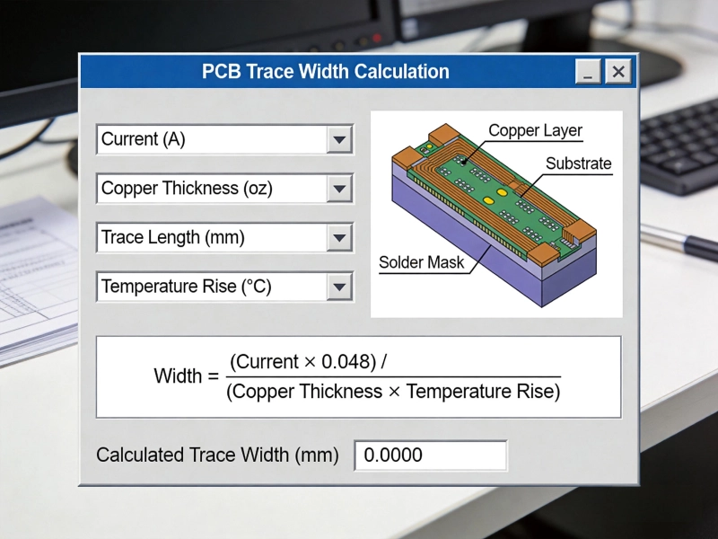
The Ipc-2221 Standard provides the most widely used formula for calculating Trace Current Capacity:
For external traces:
I = 0.048 × (ΔT)^0.44 × (A)^0.725
Where:
- I = Current in Amps
- ΔT = Temperature rise in °C
- A = Cross-sectional area in mils²
For internal traces (buried within the PCB), the current capacity is significantly reduced due to limited thermal dissipation - typically about half of external trace capacity for the same cross-section.
While the IPC formula is usefull, most designers use online calculators like the one from 4PCB or Saturn Pcb Design Toolkit. These tools account for Copper Weight, trace location (internal/external), and temperature rise to provide quick estimates.
Lets say you need to carry 20A with a 10°C temperature rise on an external trace with 1 oz copper. Using standard calculators, you'd need approximately:
If space is limited, you could use 2 oz copper, reducing the external trace width to about 200 mils. However, thicker copper increases minimum trace/space requirements and board cost by 20-40%.
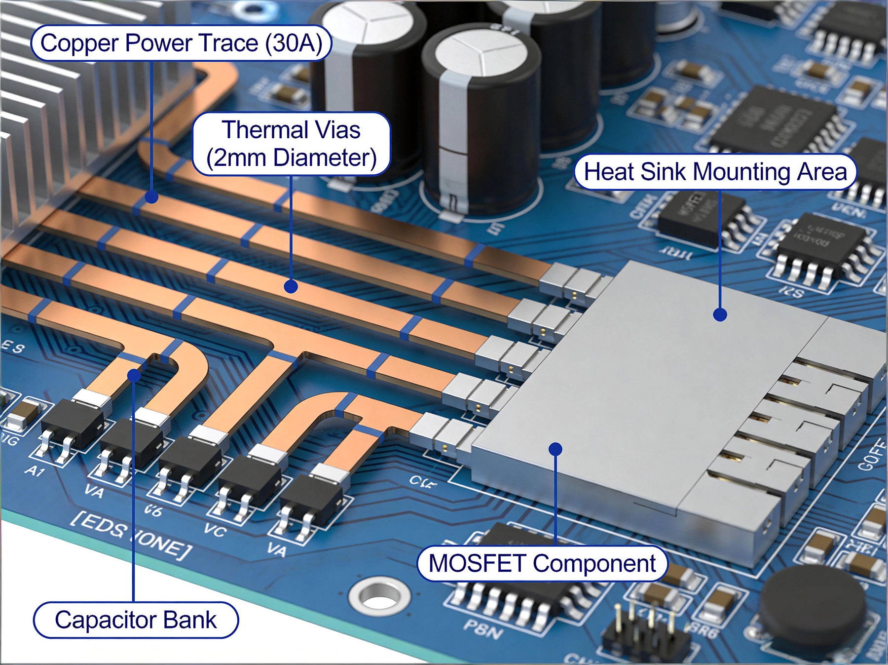
When board space is limited, consider using parallel traces or copper pours instead of a single wide trace. A Copper Pour connected to your power net can dramatically increase current capacity while also improving thermal dissipation. Pour areas act as heat spreaders, moving heat away from the trace and into the board substrate.
For multi-layer boards, you can parallel traces across layers using vias. Two 150 mil traces on different layers connected by vias can handle nearly as much current as one 300 mil trace, but with better Heat Dissipation. Just remember that vias have their own current limitations - a typical via can carry 1-2A depending on plating and diameter.
Speaking of vias, theyre often the weak link in high current paths. A standard 0.3mm via with 1 oz plating can handle about 1A with reasonable temperature rise. For higher currents, you have several options:
For a 20A current path connecting layers, we'd typically use 8-10 standard vias or 3-4 larger vias (0.6mm or greater).
High current traces generate heat, and that heat needs somewhere to go. Consider these Thermal Management strategies:
Every millimeter of trace adds resistance and inductance. In power circuits, minimize the loop area between high current paths and their return paths. This reduces both voltage drop and EMI. If your routing a motor driver, place the MOSFETs, current sense resistors, and connectors as close together as possible.
The return path is just as important as the forward path. For single-sided or 2-layer boards, route the return trace parallel and close to the forward trace. For multi-layer boards, use a dedicated ground plane on an adjacent layer. The return current naturally flows in the path of least impedance - which at high frequencies means directly under the forward trace.
High current components like connectors, MOSFETs, inductors, and diodes should be grouped together and placed near the board edge for better thermal dissipation. Avoid routing sensitive analog signals or high-speed digital traces near high current paths - the magnetic fields can cause interference.
For production testing and debugging, include test points on high current traces. These should be sized appropriately - a 1mm test point can't handle 20A for extended periods, but it's fine for brief current measurements. For ongoing current monitoring, consider dedicated current sense resistors or Hall effect sensors.
Many designers calculate trace width for exactly their required current and temperature rise, then wonder why boards fail. Always add margin - we recomend at least 30-50% extra current capacity. Manufacturing variations, environmental conditions, and component tolerances all affect real-world performance.
We've seen designs with 200 mil traces suddenly necking down to a single via, creating a thermal bottleneck. The via becomes a fuse - not a reliable connection. Always verify Via Current Capacity matches your trace requirements.
A high current trace running under a microcontroller or memory chip might not fail immediately, but the thermal stress can cause long-term reliability issues. Use thermal simulation or at least maintain generous spacing between heat sources and temperature-sensitive components.
For boards with mixed signal and power requirements, consider specifying different copper weights for different layers. Inner ground planes can be 0.5 oz while outer power layers use 2 oz. This balances cost and performance.
Modern Pcb Design tools include Thermal Analysis capabilities. Tools like Ansys Icepak, Mentor FloTHERM, or even simpler built-in solvers in Altium or KiCad can predict temperature distributions. For critical applications, thermal simulation should be part of your design verification process.
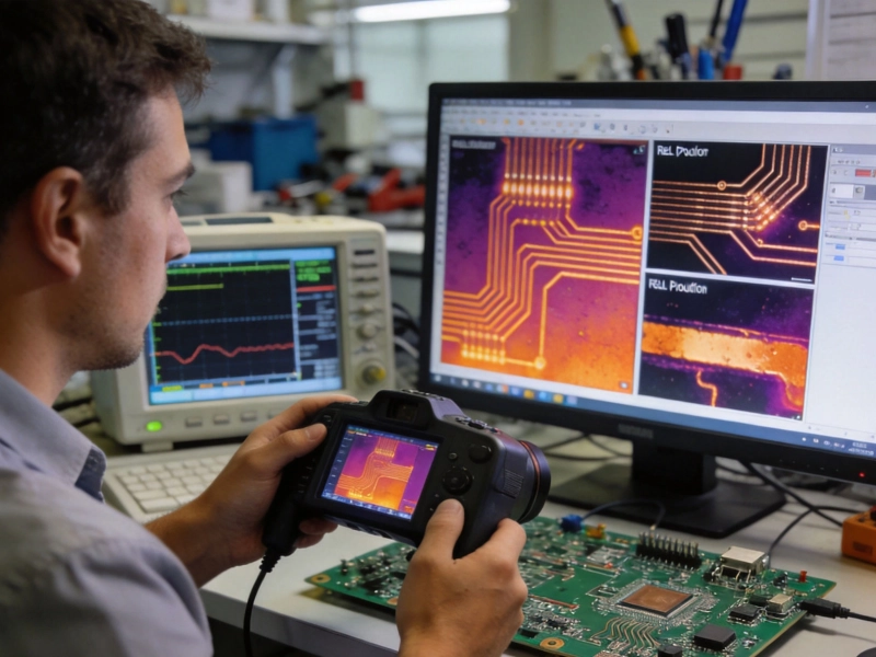
Nothing beats actual hardware testing. On prototypes, measure voltage drop across high current traces at full load using a precision voltmeter. Use a thermal camera to identify hot spots and verify temperatures stay within specifications.
Test beyond your nominal requirements. If your design needs to handle 20A, test at 25A. Test at elevated ambient temperatures. Test with worst-case component tolerances. This helps identify weak points before production.
Designing high current Pcb Traces requires a systematic approach that balances electrical requirements, Thermal Management, and practical manufacturing constraints. By understanding the relationships between current, temperature, and trace geometry, you can create reliable power delivery paths that perform consistently over your product's lifetime.
Remember these key principles:
Whether your designing a motor controller, power supply, or battery management system, these guidelines will help ensure your high current traces deliver reliable performance when it matters most.
For 10A with 1 oz copper and 10°C temperature rise, you need approximately 150 mils (3.8mm) external trace width. For internal traces, plan for about 250 mils (6.4mm).
Yes, parallel traces can work effectively and sometimes provide better thermal performance. Just ensure each trace is properly sized and they're well-connected at both ends.
Inner layer traces require more width for the same current due to limited Heat Dissipation. Use about 1.5-2x the width you'd use for external traces, and connect them to outer layer pours using Thermal Vias.
Theoretically, there's no hard maximum - it depends on available space, copper thickness, and acceptable temperature rise. Practical limits for standard PCBs are typically 50-100A with proper design. For higher currents, consider bus bars or terminal blocks.
Copper pours are generally prefered for high current applications. They provide larger cross-sectional area, better thermal dissipation, and can be more space-efficient. However, be mindful of manufacturability and avoid creating isolated copper islands.
High Current PCB Trace Width Calculator: Complete Guide with Formulas and ExamplesMay/20/2026

5 Critical Thermal Management Problems in High Power PCBsMay/21/2026
Bus bar vs PCB trace for high current: Which Solution Wins?June/16/2026
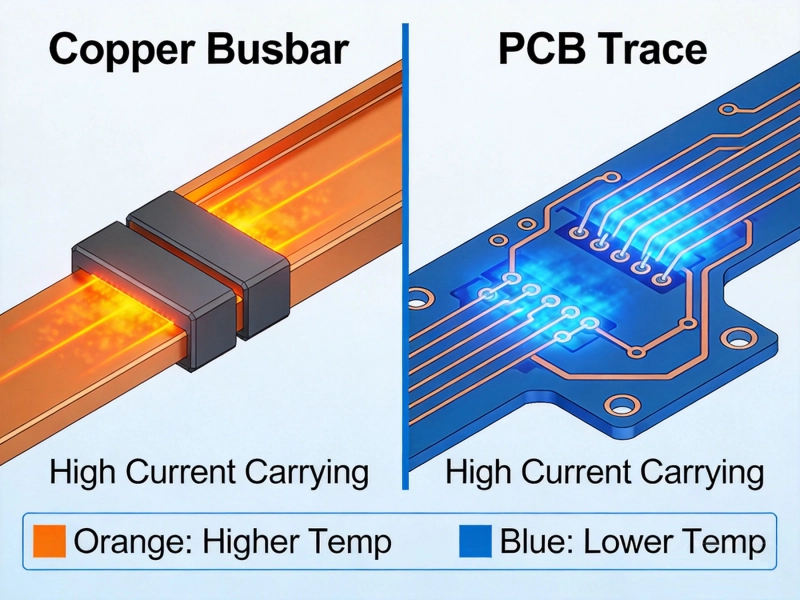
Bus Bar vs PCB Trace for High CurrentMay/21/2026
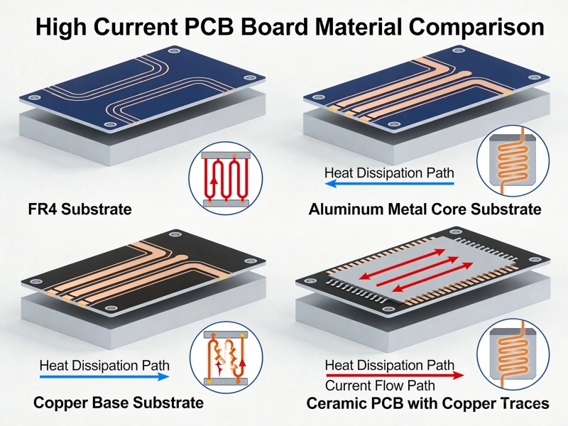
Best Material for High Current PCB Design: How to Choose the Right SubstrateJune/05/2026
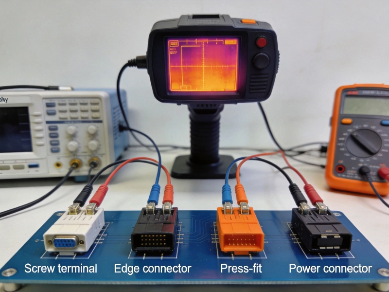
High Current PCB Connector Selection: Test Results and Real Performance DataMay/21/2026
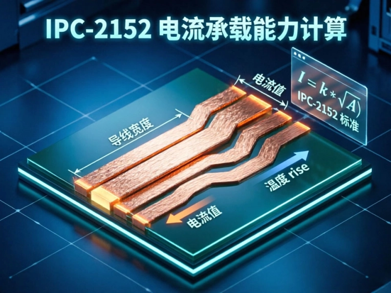
Mastering IPC-2152 Current Carrying Capacity Calculation for Reliable PCB DesignJune/04/2026
Copper Pour vs Trace: What 3 Years of PCB Failures Taught UsMay/21/2026