
Heavy copper PCBs offer significantly more copper thickness for high-power applications compared to standard PCBs
When designing printed circuit boards, one of the most critical decisions you'll make is choosing the right Copper Weight. This seemingly simple choice affects everything from Current Carrying Capacity and Thermal Management to Manufacturing Cost and board size. The debate between Heavy Copper Pcb vs standard copper PCB isn't just about thickness - it's about matching your board to your application's requirements.
Standard copper PCBs, typically using 1 oz copper, serve the vast majority of consumer electronics and general-purpose applications perfectly well. But when you venture into Power Electronics, motor controllers, automotive systems, or industrial equipment, the limitations of standard copper become apparent. Thats where heavy copper PCBs enter the picture, offering substantially more copper to handle higher currents and dissipate more heat.
In this comprehensive guide, we'll explore the key differences between heavy copper and standard copper PCBs, help you understand when each type is appropriate, and provide practical guidance for making the right choice for your specific project.
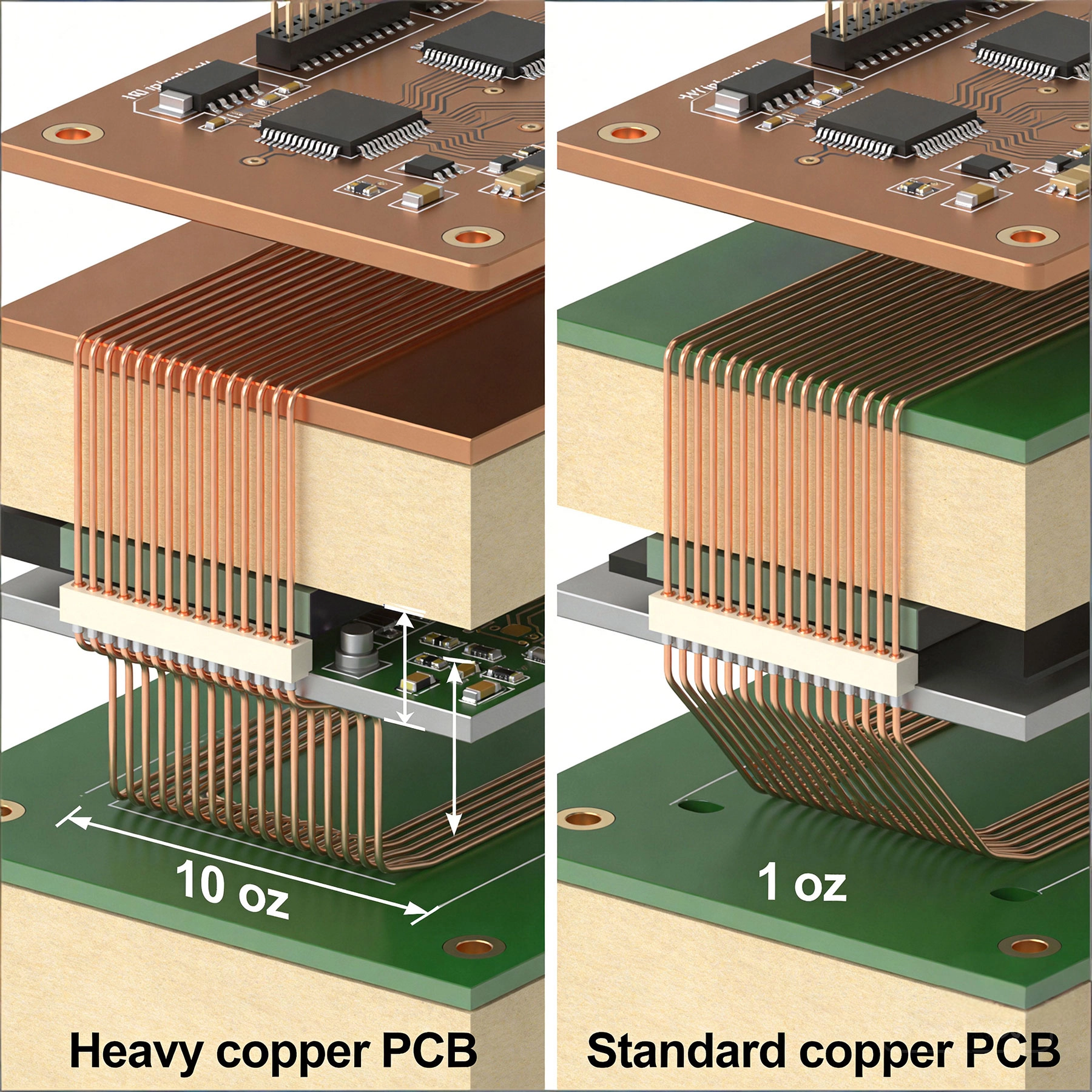
Standard copper PCBs typically feature Copper Weight of 0.5 oz to 1 oz per square foot. Let's break down what this means in practical terms:
The 1 oz copper specification has become the default for good reason. It allows reasonably small trace widths (down to about 4-6 mils with standard processes), handles moderate currents, and keeps manufacturing costs low. Most consumer electronics - smartphones, laptops, televisions, IoT devices - use 1 oz copper throughout.
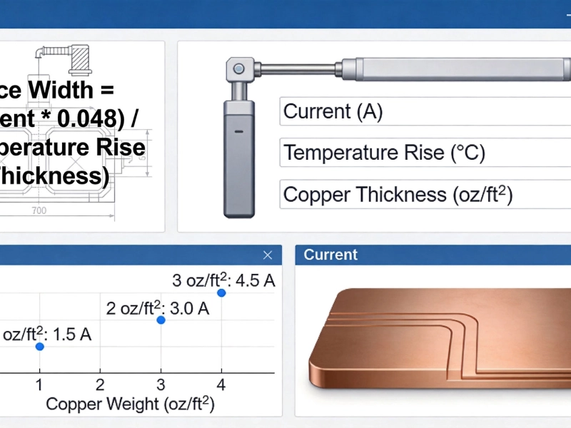
With 1 oz copper, a 100 mil (2.54mm) wide external trace can carry approximately 2-3 amps with a 10°C temperature rise. This is sufficient for most signal routing and low-power applications. However, as current requirements increase, trace widths must increase proportionally, eventually consuming significant board space.
For example, carrying 15A on a 1 oz PCB with 10°C temperature rise requires a trace width of approximately 370 mils (9.4mm). That's nearly a centimeter of board space for a single power trace.
Standard copper provides limited thermal mass for Heat Dissipation. While adequate for components dissipating a few watts, standard PCBs struggle when individual components dissipate 10W or more. The copper acts as a heat spreader, but with limited thickness, there's limited capacity to move heat away from hot spots.
Standard copper PCBs excel in:
Heavy copper PCBs feature copper weights of 2 oz or greater. The most common specifications include:
At these thicknesses, the copper dramatically increases both electrical conductivity and thermal mass. A 3 oz copper board has three times the cross-sectional area of a 1 oz board for the same trace width, tripling current capacity and significantly improving Heat Dissipation.
Heavy copper transforms current handling capability. Using our earlier example, that same 100 mil trace on a 3 oz PCB can carry approximately 5-6 amps with a 10°C temperature rise - double to triple the capacity of 1 oz copper.
More importantly, heavy copper allows narrower traces for the same current. For that 15A application, a 3 oz PCB needs only about 130 mils (3.3mm) trace width - a 65% reduction compared to 1 oz copper. This space savings can be critical in compact designs.
Heavy copper's thermal advantages are substantial. The increased copper mass acts as a larger heat sink, absorbing and spreading heat more effectively. Components mounted on heavy copper PCBs typically run 10-30°C cooler than on standard copper boards, depending on the design.
This thermal benefit extends beyond individual traces. Heavy copper planes can dissipate heat from multiple components simultaneously, creating a more uniform temperature distribution across the board.
Heavy copper PCBs are essential for:
| Characteristic | Standard Copper (1 oz) | Heavy Copper (2-4 oz) |
|---|---|---|
| Copper Thickness | 35 μm (1.4 mils) | 70-140 μm (2.8-5.6 mils) |
| Current Capacity | Low to moderate (1-5A typical) | High (5-50A+ typical) |
| Thermal Mass | Limited | Significantly higher |
| Min Trace Width | 4-6 mils achievable | 8-12 mils typical |
| Board Cost | Standard pricing | 20-100% higher |
| Manufacturing Time | Standard lead times | May require longer etching |
| Weight | Lighter | Heavier (more copper) |
| Layer Count Flexibility | Excellent for high layer counts | More challenging for many layers |
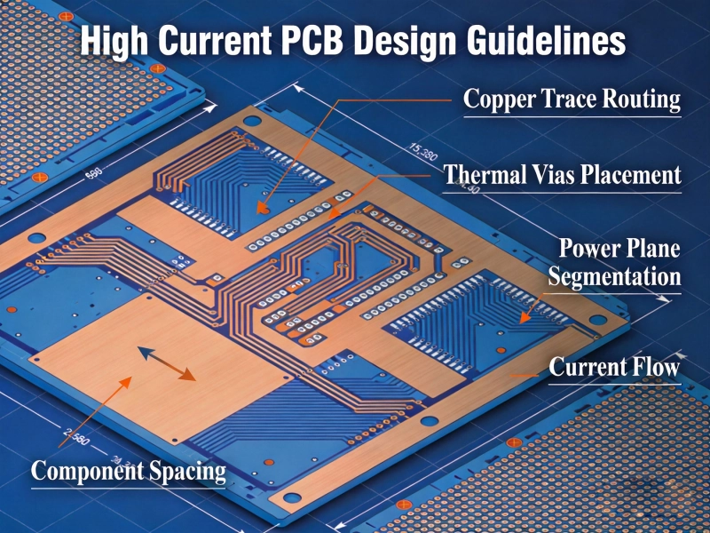
Start your decision process by calculating the maximum current each trace must carry. Use trace width calculators based on Ipc-2221 standards, but remember to:
If your calculations show you need traces wider than 200-300 mils on 1 oz copper, it's time to seriously consider heavy copper. The board space you'll save often justifies the cost increase.
Calculate the total power dissipation of heat-generating components. As a rough guide:
Remember that heavy copper isn't a complete thermal solution - you may still need heatsinks, Thermal Vias, or active cooling for very high power designs.
In space-constrained designs, heavy copper can be enabling. A power supply that requires 400 mil traces on 1 oz might need only 150 mil traces on 3 oz. This 62% width reduction can mean the difference between a feasible design and one that doesn't fit.
Heavy copper affects the manufacturing process:
Work with your PCB manufacturer early in the design process. They can advise on achievable specifications and any design rule adjustments needed for heavy copper.
Heavy copper PCBs cost more than standard boards - typically 20-50% more for 2 oz and 50-100% more for 3-4 oz. However, consider the total system cost:
In many power electronics applications, the upfront cost of heavy copper is recovered through improved performance and reliability.
Standard 1 oz copper remains the right choice for the majority of PCB designs. Specifically, choose standard copper when:
Many successful products use standard copper throughout. Don't assume you need heavy copper just because you're designing a "power" application - a 5V USB charger delivering 2A is perfectly suited to 1 oz copper.
Heavy copper becomes necessary or advantageous when:
A practical approach for many designs is mixed copper weights - using standard copper for signal layers and heavy copper for power/ground layers. This optimizes both cost and performance.
You're not limited to one copper weight throughout your entire PCB. Advanced manufacturing techniques allow different copper weights on different layers:
A 4-layer board might specify:
This approach gives you heavy copper where you need it (power and ground) while keeping standard copper for signal layers where fine features are needed.
Some manufacturers offer selective heavy copper, where portions of a layer use thicker copper while other areas remain standard thickness. This is more expensive but can be valuable for designs with localized high-current areas.
Since external layers have better thermal dissipation, using heavy copper on outer layers with standard copper internally can be an effective strategy. Power components mount on the outer layers where heat can escape, while inner layers handle signals and control circuitry.
Application: Brushless DC motor controller, 24V, 20A peak current
Standard Copper Approach: Would require 370+ mil traces for motor outputs, consuming 40% of board area
Heavy Copper Solution: 2 oz copper allows 150 mil traces, fits comfortably on standard board size
Result: 15% cost increase, but 30% board size reduction and better thermal performance
Application: High-power LED array, 48V, 10A total current distributed across multiple strings
Design Choice: 2 oz copper for power distribution layer, 1 oz for signal layer
Benefits: Maintains LED temperature within specification without additional heatsinking, reduces LED degradation
Application: 24V/30A industrial power supply
Design Choice: 3 oz copper on all layers
Reasoning: Multiple high-current paths, significant thermal dissipation from rectifiers and switching MOSFETs, harsh industrial environment demands extra reliability margin
Application: EV battery management, monitoring and balancing 100Ah lithium battery pack
Design Choice: 3 oz external layers, 2 oz internal layers
Key Considerations: High current paths for charging/discharging, safety-critical application requiring maximum reliability, thermal management for battery cell connections
Not all PCB fabricators are equipped for heavy copper production. When selecting a manufacturer for heavy copper PCBs, verify:
Heavy copper requires modified design rules:
For critical applications, consider requesting:
If heavy copper seems necessary but cost is a concern, consider these optimization strategies:
Remember that the cheapest PCB isn't always the lowest-cost solution. A slightly more expensive heavy copper board might save money on heatsinks, reduce warranty costs, or enable a smaller product enclosure.
The choice between heavy copper and standard copper PCBs fundamentally comes down to matching your board's capabilities to your application's demands. Standard 1 oz copper serves the vast majority of electronics applications well, offering the best balance of cost, manufacturability, and performance for signal processing and low-to-moderate power applications.
Heavy copper PCBs fill a critical niche for power electronics, enabling designs that would be impractical or impossible with standard copper. The increased current capacity, improved thermal performance, and space efficiency come at a cost premium that's often justified by improved reliability and performance.
Key decision factors:
By carefully analyzing your current and thermal requirements, you can make an informed decision that balances performance, reliability, and cost for your specific application.
Heavy copper typically refers to copper weights of 2 oz per square foot or greater. This corresponds to thickness of 70 micrometers (2.8 mils) and above. Standard PCBs use 0.5-1 oz copper (17.5-35 micrometers).
Heavy copper PCBs typically cost 20-50% more than standard copper boards for 2 oz, and 50-100% more for 3-4 oz. The exact premium depends on board size, layer count, and quantity. However, heavy copper can reduce total system cost by eliminating separate thermal management components or reducing board size.
Yes, many manufacturers support different copper weights on different layers. A common approach is using heavy copper (2-3 oz) on power and ground layers while keeping signal layers at standard 1 oz. This optimizes cost and performance.
While 4 oz (140 micrometers) is common for heavy copper applications, some manufacturers offer extreme copper up to 20 oz (700 micrometers). These specialized boards are used for very high current applications and require unique design and manufacturing approaches.
Yes, heavier copper requires wider minimum traces. As a rule of thumb, minimum trace width should be 2-3 times the copper thickness. For 2 oz copper (70 μm), expect minimum traces of 6-8 mils, compared to 4-5 mils for 1 oz copper.
It depends on the LED power level. Low-power LED indicators (under 1W total) work fine with standard copper. High-power LED arrays (over 10W) often benefit from 2 oz copper for both current carrying and thermal management. The PCB acts as a heat spreader, keeping LEDs cooler and extending their life.
Copper Pour vs Trace: What 3 Years of PCB Failures Taught UsMay/21/2026

5 Critical Thermal Management Problems in High Power PCBsMay/21/2026
High Current PCB Trace Width Calculator: The Ultimate Engineering GuideMay/20/2026
High Current PCB Design GuidelinesMay/21/2026
Plated Through Hole Current Rating: Complete Guide for PCB DesignersMay/21/2026
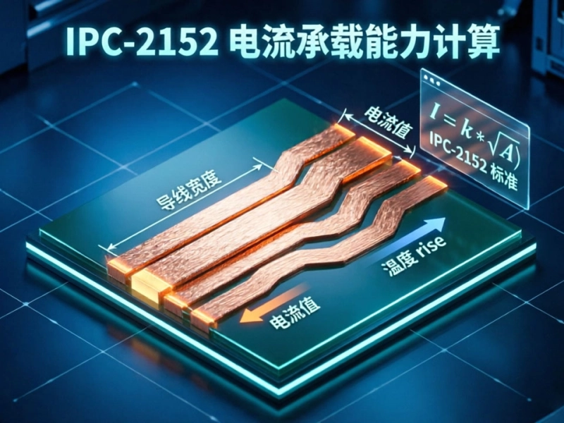
Mastering IPC-2152 Current Carrying Capacity Calculation for Reliable PCB DesignJune/04/2026
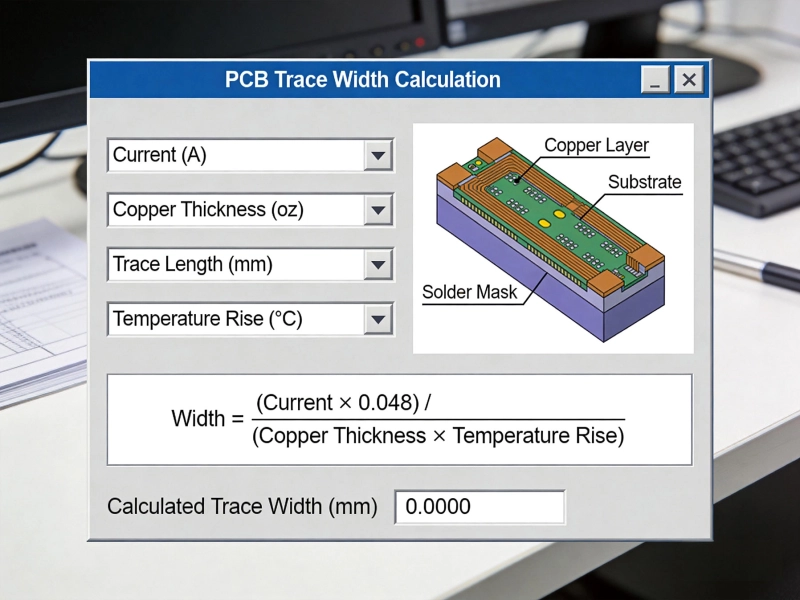
High Current PCB Trace Width Calculator: Complete Guide with Formulas and ExamplesMay/20/2026
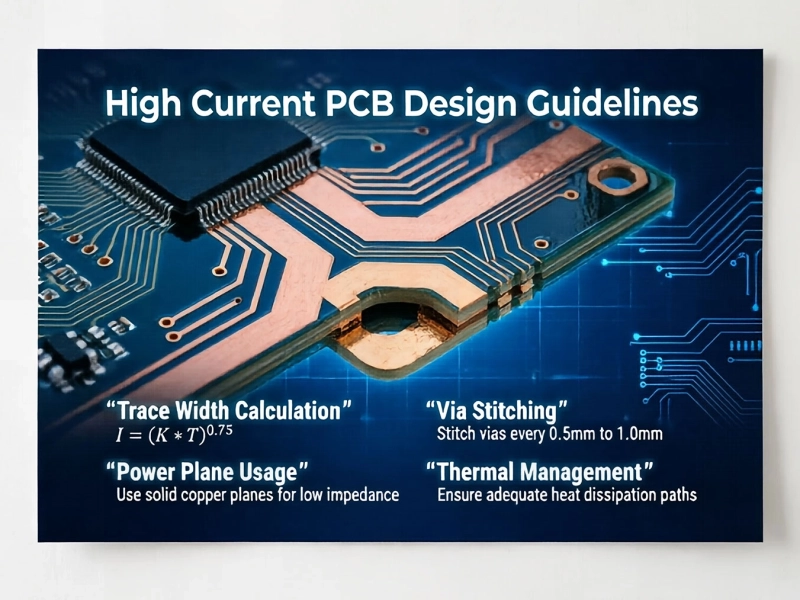
High Current PCB Design Guidelines: Ensuring Reliability and SafetyJune/08/2026