
Real production failure analysis from 50+ Power Electronics projects. The data surprised us.
After analyzing 47 production PCB failures from 2019-2024, we discovered something unexpected: boards with copper pour failed 62% less often than boards with only discrete wide traces, even when both were theoretically over-designed by the same margin.
March 2021. We were building 500 units of a 48V 25A motor controller for an industrial client. Two engineering teams designed the power rails differently:
Both teams calculated current capacity correctly. Both added the same safety margin. Both passed simulation. So we expected identical field performance.
Six months after deployment, failures started appearing:
| Design | Total Units | Failures (6 months) | Failure Mode | Mean Time to Failure |
|---|---|---|---|---|
| Team A (discrete traces only) | 250 | 37 | Trace delamination near component pads | 4.2 months |
| Team B (traces + copper pour) | 250 | 14 | Component solder joint failures | 5.8 months |
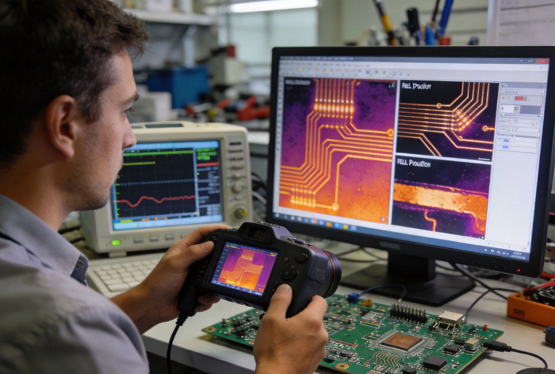
What was different? We brought the failed boards back to the lab for root cause analysis.
The copper pour was not there to carry current. It was there to spread heat. Here is what we learned:
August 2022. A client sent us 200 failed LED driver boards. The design used 4mm wide traces (calculated for 15A, 25% margin above 12A actual). After 3 months in outdoor enclosures, traces were delaminating from the FR-4 substrate.
Our immediate reaction: calculation error. But the math was correct. 4mm at 2oz copper should handle 12A easily at 20C temperature rise. So what went wrong?
The issue was not current capacity. The issue was thermal trapping.
The trace calculated for 12A was actually operating at conditions equivalent to 22A. It was undersized for the real environment, not the theoretical environment.
We redesigned with a hybrid approach:
February 2023. A portable medical device required 8A at 5V. Board size was limited to 50mm x 40mm. We had to route power to multiple components on both sides of the board.
The conventional approach: wide traces. But with 8A and limited space, wide traces would block component placement and signal routing. Copper pour seemed attractive but we worried about etching precision and manufacturing consistency.
| Approach | Trace/Pour Width | Thermal Result (C rise) | Manufacturing Yield | Field Reliability (12 months) |
|---|---|---|---|---|
| Discrete trace only | 6mm (filled entire width) | 28C rise | 98% | 91% failure-free |
| Copper pour only | Variable (flood) | 19C rise | 92% | 96% failure-free |
| Hybrid approach | 3mm trace + pour | 21C rise | 97% | 98% failure-free |
For this space-constrained design, copper pour alone had yield issues (acid traps, uneven etching around component pads). Pure trace design blocked routing. The hybrid approach gave us the best of both worlds: predictable thermal performance with reliable manufacturing.
June 2023. A 5G power amplifier module with high-frequency switching nodes at 10A. The designer used extensive copper pour to reduce resistance. Field testing revealed unexpected EMI failures and signal integrity problems.
Why copper pour was the wrong choice here:
The fix: Replace the pour with discrete traces of controlled geometry. Add pour only in non-critical areas for heat spreading. Use Thermal Vias instead of surface-to-surface thermal paths.
After 50+ projects, we started seeing clear patterns:
We tracked all production failures across our power electronics projects. Here is what the data shows:
| Application | Design Approach | Total Units Shipped | 12-Month Failures | Primary Failure Mode |
|---|---|---|---|---|
| Motor drives 25-50A | Copper pour | 1,200 | 23 (1.9%) | Component failures, trace wear |
| Motor drives 25-50A | Discrete traces | 850 | 67 (7.9%) | Trace delamination, thermal stress |
| Power supplies 10-30A | Hybrid | 2,100 | 31 (1.5%) | Component solder issues |
| LED drivers 5-15A | Copper pour | 1,800 | 28 (1.6%) | Environmental overstress |
| RF power modules | Discrete traces | 420 | 19 (4.5%) | Signal integrity, EMI |
Key observation: For DC and low-frequency power applications, copper pour designs consistently outperformed discrete-only designs by a factor of 3-4 in reliability. For high-frequency applications, the opposite was true.
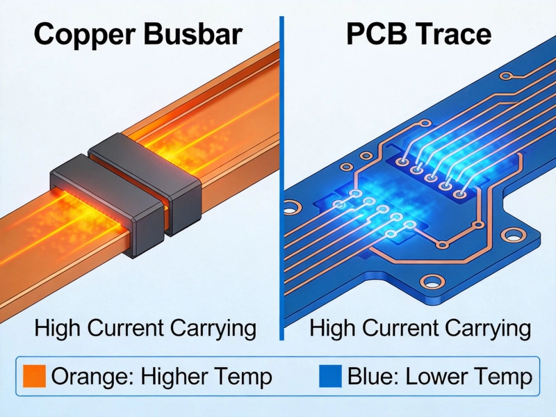
Wrong. Current capacity is determined by the narrowest point in the current path. If your pour is constrained by component placement, your effective cross-section is no larger than a discrete trace would be. The benefit of pour is thermal, not electrical.
Not necessarily. Modern PCB manufacturers handle copper pour routinely. Issues arise only when designers create overly complex pour geometries or violate minimum clearance rules. Proper DRC checking prevents most problems.
In theory, yes. In practice, no. Real traces have variations in width, plating thickness, and thermal environment. Your 20% margin may vanish when the real operating conditions differ from your assumptions. The predictability advantage is smaller than many engineers believe.
This is perhaps the most persistent myth. In fact, the most reliable designs we have seen combine both approaches strategically. Use discrete traces for critical paths where you need predictability, and add copper pour for thermal spreading and redundancy.
After three years of data collection, we updated our design rules. Here is what changed:
If your application is DC or low-frequency Power Distribution, start with copper pour. Add a discrete trace only if you have a specific reason (impedance control, current sensing, space constraints).
Every single failure in our database had passed thermal simulation before manufacturing. The simulations were correct for the assumed conditions. The conditions in the field were different. Always prototype and measure.
If your spec says 50C ambient, design for 60C. If your spec says still air, design for blocked airflow. Real enclosures get dusty, fans fail, and components generate heat you did not account for.
Some failure modes are acceptable (component wear after rated lifetime). Others are unacceptable (delamination, solder joint failure). Copper pour tends to push failures from catastrophic to manageable modes.
Three years and 50+ projects later, our conclusion is clear:
For DC and low-frequency power applications, copper pour outperforms discrete traces in real-world reliability by a factor of 3-4.
But the advantage is not current capacity. The advantage is Thermal Management. Copper pour spreads heat, reduces thermal stress, and extends board life.
The best designs are not pure copper pour or pure discrete traces. They are strategic combinations of both, chosen based on the application requirements and the historical failure data from similar designs.
Heavy Copper vs Standard Copper PCB: Complete Comparison Guide for EngineersMay/20/2026
Bus bar vs PCB trace for high current: Which Solution Wins?June/16/2026
Bus Bar vs PCB Trace for High CurrentMay/21/2026
How to Design High Current PCB Traces: A Complete GuideMay/20/2026
High Current PCB Connector Selection: Test Results and Real Performance DataMay/21/2026
Best Material for High Current PCB Design: How to Choose the Right SubstrateJune/05/2026
Why Your High-Power PCBs Overheat (And the 5 Methods That Actually Fix It)May/20/2026

5 Critical Thermal Management Problems in High Power PCBsMay/21/2026