
Everything you need to know about PCB Via Current Capacity, thermal limits, and design optimization
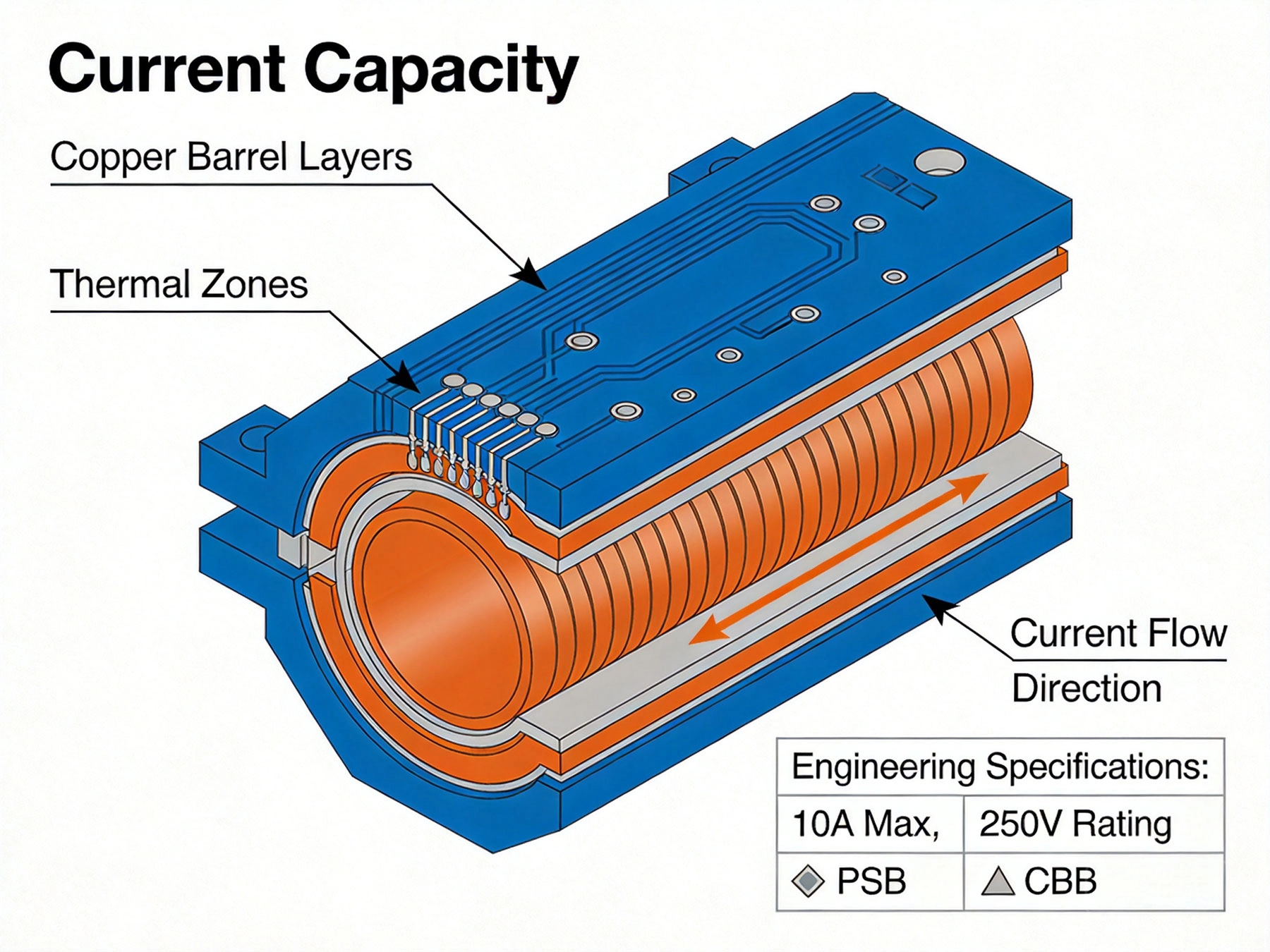
A plated through hole (PTH) via is more than just a hole in your PCB. It is a cylindrical copper barrel connecting layers, and when current flows through a via, it travels through this copper barrel. The resistance of that barrel determines both voltage drop and heat generation.
The critical misconception many engineers have: vias are just connections. Wrong. Vias are resistors, and at high currents, they are thermal liabilities. Understanding Plated Through Hole Current Rating is essential for any Power Electronics Design.
Current in a via barrel flows along the cylindrical copper wall. The effective cross-sectional area is the circumference times the plating thickness:
Where: D = drill diameter, t = plating thickness
For a 0.5mm drill with 25 micrometers plating:
Key insight: A single 0.5mm via has less than half the cross-sectional area of a modest power trace. This is why vias limit current capacity.
Vias have two distinct current limits:
| Limit Type | What It Means | Typical Threshold |
|---|---|---|
| Electrical Limit | Voltage drop becomes unacceptable | Usually 10-50mV per via |
| Thermal Limit | Temperature rise damages the board | Usually 10-20 degrees C rise |
In practice, thermal limits govern for most designs. A via that works electrically may still fail thermally by melting solder or delaminating the board.
Note: These values assume 1oz (25 micrometers) finished copper plating, 20 degrees C ambient, still air, and no thermal relief. Your actual results may vary based on PCB construction and thermal environment.
| Plating Weight | Finished Thickness | 0.5mm Via Capacity | 0.8mm Via Capacity |
|---|---|---|---|
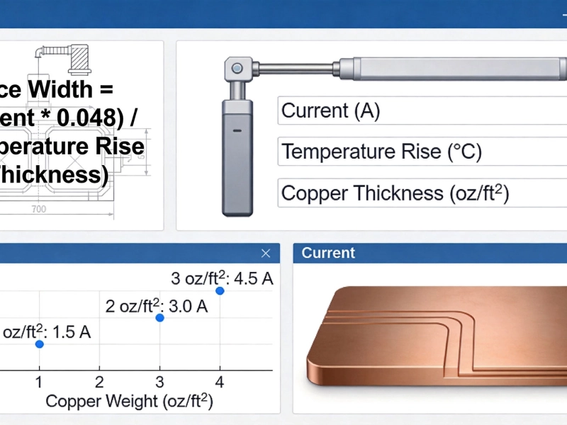
| 0.5 oz (HALT) | ~12 micrometers | 4A | 8A |
| 1 oz (standard) | ~25 micrometers | 8A | 15A |
| 2 oz | ~50 micrometers | 14A | 26A |
| 3 oz | ~75 micrometers | 20A | 38A |
IPC standards allow plating thickness to vary. Minimum spec might be 0.7 mil (18 micrometers) while the average is higher. Always design for minimum plating thickness unless your manufacturer guarantees otherwise.
Where: rho = copper resistivity (1.7x10^-8 ohm-m), L = board thickness, A = barrel cross-section
| Via Size | Board Thickness | Resistance | Voltage Drop at 10A |
|---|---|---|---|
| 0.5mm drill | 1.6mm | ~1.1 mOhm | 11 mV |
| 0.8mm drill | 1.6mm | ~0.5 mOhm | 5 mV |
| 1.0mm drill | 1.6mm | ~0.25 mOhm | 2.5 mV |
For a 48V power bus with 10 vias carrying 20A:
Countless designs fail because engineers underestimated via current demands. Here is what happens:
Spread current across multiple smaller vias:
Fill vias with conductive epoxy or solid copper:
| Filling Type | Current Capacity Gain | Cost Impact | Best For |
|---|---|---|---|
| Standard (empty) | 1x baseline | Baseline | Low current |
| Conductive epoxy fill | 1.5-2x improvement | +30-50% | Medium current |
| Copper overplate fill | 2-3x improvement | +80-100% | High Current |
| Solid copper (metal coin) | 5-10x improvement | +200%+ | Extreme current |
For production reliability, tenting or covering vias prevents solder wicking:
But be careful - tented vias can trap air during thermal cycling, causing reliability issues in high-temperature applications.
Place vias directly in component pads:
Step 1: Determine via requirements
Single 0.5mm via at 10A = 8A capacity (from table)
Need: 20A / 8A = 2.5 vias minimum
Step 2: Add safety margin (50%)
2.5 x 1.5 = 3.75, round up to 4 vias minimum
Step 3: Choose via arrangement
4 x 0.5mm vias in 2x2 array, 1mm spacing
Step 4: Verify trace width to via transition
Each via needs 100mil pad minimum = 4 x 100mil = 400mil trace width capacity
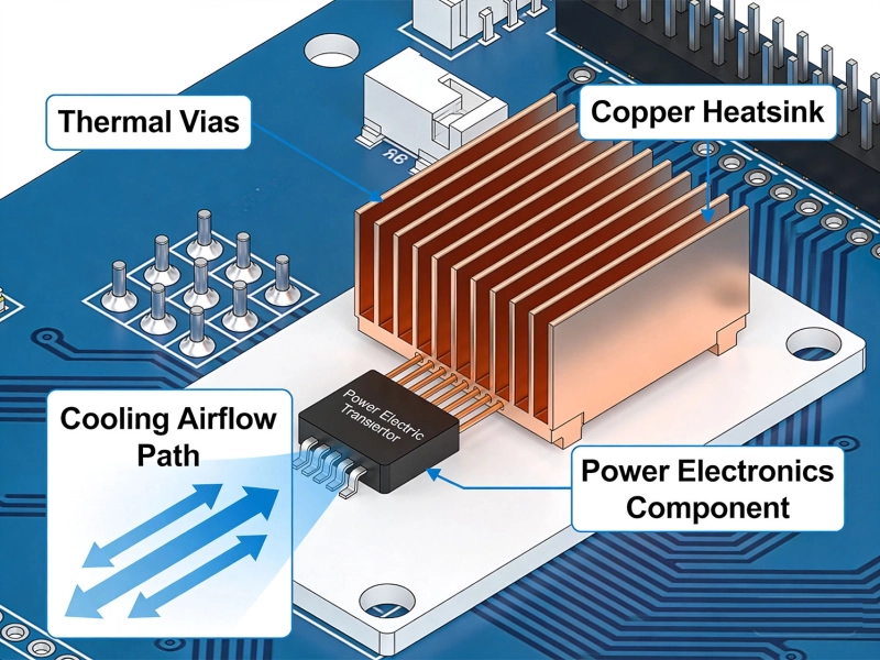
Power MOSFETs with thermal pads often require dozens of Thermal Vias:
High-power modules need specialized approaches:
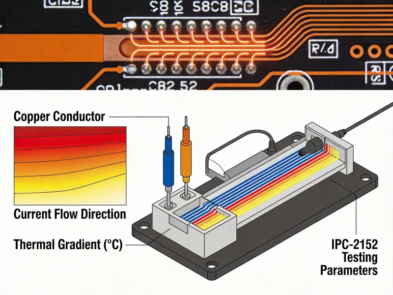
A via heats up due to I2R losses in the copper barrel. The heat must escape through:
A via surrounded by copper planes will run cooler than one in bare FR-4. Always connect high-current vias to inner copper planes with thermal via arrays.
For quick estimation without simulation:
Where: h = convective heat transfer coefficient (~100 W/m2-K), A = surface area
This is an approximation. For critical designs, use thermal simulation or physical testing.
| Parameter | IPC-A-600 Class 2 | IPC-A-600 Class 3 |
|---|---|---|
| Minimum annular ring | 2 mil (0.05mm) | 5 mil (0.13mm) |
| Voiding in barrel | less than 10% | less than 5% |
| Minimum drill size | 0.25mm (10mil) | 0.3mm (12mil) |
Before production, verify Via Current Capacity with:
| Current Range | Recommended Approach | Example Configuration |
|---|---|---|
| 0-3A | Single standard via | 1 x 0.4mm via |
| 3-8A | Single larger via | 1 x 0.8mm via, or 2 x 0.5mm |
| 8-15A | Via array | 3-4 x 0.5mm vias in array |
| 15-30A | Via array + thermal planes | 6-8 x 0.5mm + inner plane connection |
| 30-50A | Filled vias + heavy copper | 8-12 x 0.8mm filled + 2oz copper |
| 50A+ | Copper coins or busbars | Specialized construction required |
Manufacturer current ratings assume ideal conditions. Real boards have thermal gradients, non-uniform plating, and manufacturing variations. Always add margin.
A 1mm via in a 0.5mm pad creates a stress concentration. Pad diameter should be minimum 2x drill diameter.
CTE mismatch between copper and FR-4 causes via barrel cracks over time. This is accelerated at high temperatures and high currents.
Blind vias are harder to plate uniformly and more expensive. Use through-hole vias for Power Distribution unless space absolutely requires otherwise.
Start with conservative estimates, prototype with thermal imaging, and always verify before committing to production. The cost of a via redesign is trivial compared to field failures.
IPC-2152 Current Carrying Capacity Calculation GuideJune/03/2026
High Current PCB Trace Width Calculator: The Ultimate Engineering GuideMay/20/2026

5 Critical Thermal Management Problems in High Power PCBsMay/21/2026
Why Your High-Power PCBs Overheat (And the 5 Methods That Actually Fix It)May/20/2026
High Current PCB Design GuidelinesMay/21/2026
High Current PCB Design Guidelines: Ensuring Reliability and SafetyJune/08/2026
Mastering IPC-2152 Current Carrying Capacity Calculation for Reliable PCB DesignJune/04/2026
Best Material for High Current PCB Design: How to Choose the Right SubstrateJune/05/2026