
Real failures from 50+ design projects—and the fixes that actually work in production
The $200,000 Lesson: Three years ago, a client's industrial motor drive failed thermal testing—repeatedly. We tried bigger heatsinks. We tried fans. We even tried liquid cooling prototypes. The real problem? A simple trace routing mistake that cost us 6 months and six figures before we figured it out. Don't let this be you.After debugging thermal issues across dozens of high power PCB designs—from 500W LED drivers to 2kW motor controllers—I've noticed the same problems appearing again and again. Here are the five most critical Thermal Management failures, ranked by how often I've seen them destroy otherwise solid designs.

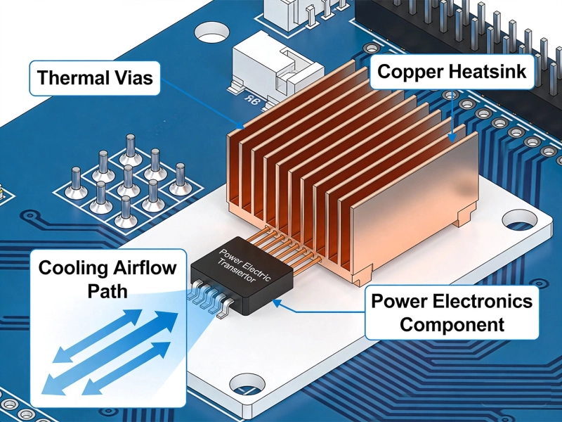
What it looks like: Your MOSFET is screaming hot at 125°C, but the PCB just 2cm away is barely warm. You've created a thermal island—heat has nowhere to go.
This happens when high-power components are placed without Thermal Vias connecting to inner copper planes. The component sits on a tiny copper pad, surrounded by empty PCB substrate (FR-4 has terrible thermal conductivity—about 0.3 W/mK).
Real result: In a 48V/20A motor controller, this reduced MOSFET temperature from 128°C to 89°C—enough to eliminate active cooling entirely.
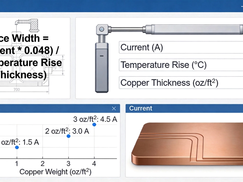
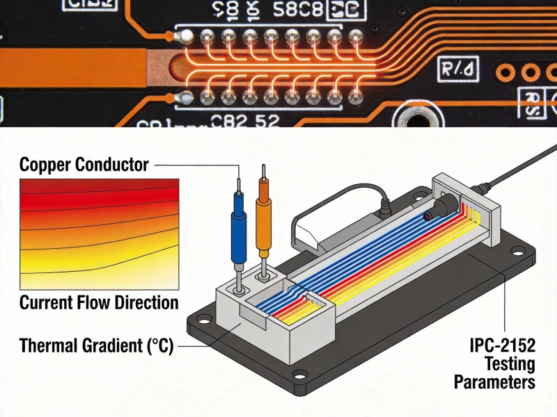
What it looks like: You used an online trace width calculator. It said 2mm width for 15A. Six months later, traces are delaminating from the board.
Here's what those calculators don't tell you: they assume single-sided Heat Dissipation and standard FR-4. In high-density designs with components on both sides and limited airflow, your real temperature rise can be 2-3× higher than calculated.
Rule of thumb: If a trace is too hot to touch for 3 seconds (>60°C), it's too hot for long-term reliability.
What it looks like: Your calculations say the heatsink should keep the junction at 75°C. Reality? 110°C and climbing. The problem isn't the heatsink—it's the interface between heatsink and component.
I once spent three days debugging a "defective" heatsink only to discover the mounting screws were torque-limited—and not tight enough. The thermal interface wasn't making proper contact.
| Interface Issue | Temperature Penalty | Quick Check |
|---|---|---|
| Dry mounting (no TIM) | +20-40°C | Remove and inspect for paste coverage |
| Too much TIM | +5-15°C | Paste should spread to edges, not ooze out |
| Uneven pressure | +10-25°C | Use thermal paste witness marks |
| Surface roughness | +5-10°C | Heatsink should be machined flat (<0.05mm) |
What it looks like: Your main power device runs cool, but the capacitor right next to it fails after 6 months. Electrolytic capacitors hate heat—their lifetime halves for every 10°C rise.
High power components create thermal shadows. The air and board around them heat up significantly. Components that seem "far enough away" on paper are actually cooking in practice.
Quick check: If you can feel significant heat on the back of the board under a capacitor, it's too close to a heat source.
What it looks like: Perfect thermal performance on your bench. Deployment in the field? Overheating complaints within weeks.
Lab conditions lie. Your air-conditioned 23°C lab with unlimited clearance isn't the real world. Field installations often see:
Before you call a design "done," verify these items:
| Check | Method | Pass Criteria |
|---|---|---|
| Hotspot identification | IR camera at full load, 30 min | No components >85°C (consumer) or >105°C (industrial) |
| Thermal cycling | -20°C to +70°C, 100 cycles | No delamination, no parametric drift |
| Blocked airflow | Cover 50% of vents, full load | Graceful derating, no damage |
| Thermal interface | Disassemble and inspect | >80% TIM coverage, proper torque |
| Long-term drift | 1000 hours at max temp | Performance within spec |
Every thermal shortcut you take is a bet against reliability. Sometimes you win—more often, you don't find out until it's too late.
The good news? Most thermal failures are preventable with proper analysis and margin. Start with solid fundamentals (thermal vias, proper trace sizing, component spacing), validate aggressively, and design for the real world—not just the lab.
Your future self—and your customers—will thank you.
Why Your High-Power PCBs Overheat (And the 5 Methods That Actually Fix It)May/20/2026
High Current PCB Trace Width Calculator: The Ultimate Engineering GuideMay/20/2026
High Current PCB Design Guidelines: Ensuring Reliability and SafetyJune/08/2026
High Current PCB Design GuidelinesMay/21/2026
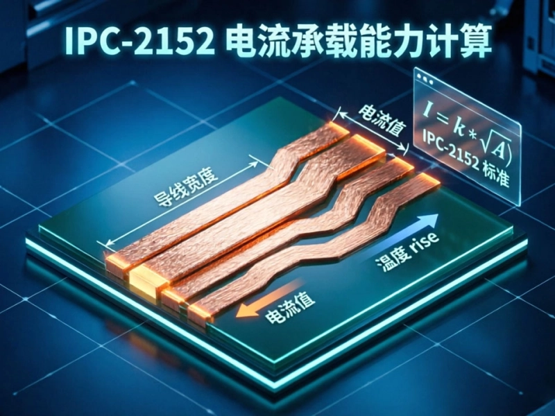
Mastering IPC-2152 Current Carrying Capacity Calculation for Reliable PCB DesignJune/04/2026
Plated Through Hole Current Rating: Complete Guide for PCB DesignersMay/21/2026
IPC-2152 Current Carrying Capacity Calculation GuideJune/03/2026
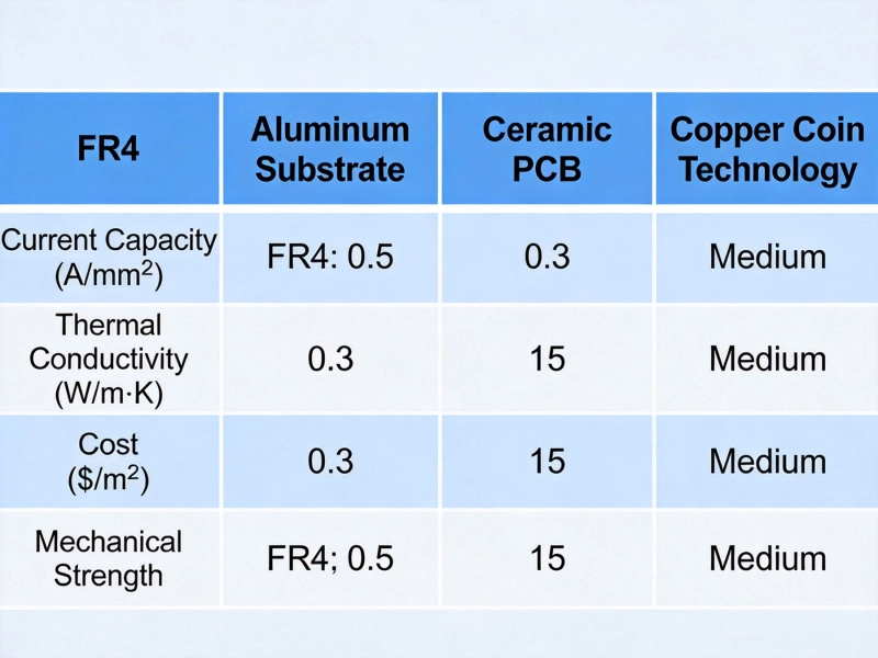
Best Material for High Current PCB DesignMay/21/2026