

Power Electronics push current levels that consumer gadgets never encounter. When amperage climbs past 5A, 10A, or even 100A, the humble solder joint becomes a critical design element. Get it wrong, and you face field failures, thermal runaway, or safety hazards.
If you're designing high-current PCBs, the choice between wave soldering and selective soldering affects more than just production efficiency—it impacts joint reliability, thermal performance, and whether your Power Electronics survive real-world conditions.
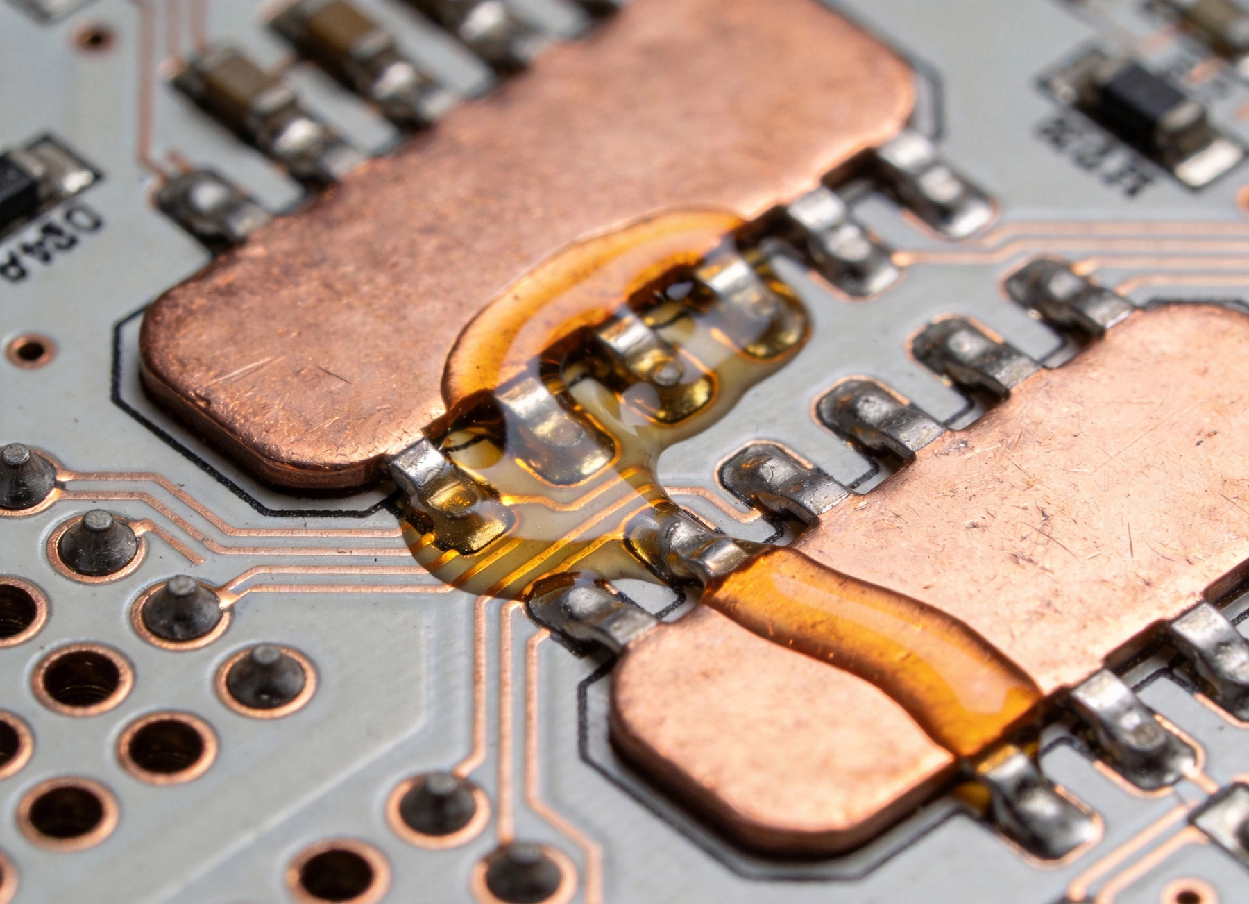
Regular signal joints care about connectivity and some mechanical strength. High-current joints care about sustained Current Carrying Capacity, Thermal Management, and long-term reliability under load cycling.
A typical 0.5mm solder joint on a SOIC package handles milliamps comfortably. But a solder joint for a Bus Bar termination carrying 50A demands entirely different engineering thinking. The joint must:
The soldering process directly affects all four requirements.
Wave soldering has long served high-current through-hole components. Power transistors, electrolytic capacitors, and heavy connectors routinely pass through wave solder lines. The bulk process delivers consistent fillet formation across many joints simultaneously.
Wave soldering handles large component leads effectively. Thick copper component leads and heavy terminals absorb heat during wave contact without suffering damage. The solder fills through-holes thoroughly, creating robust fillets that resist mechanical stress.
The high thermal mass of wave solder pots maintains stable temperatures even when processing large, cold boards. You don't get the temperature drop that small selective solder pots might experience with intermittent production runs.
Power supplies commonly use wave soldering for main filter capacitors, bridge rectifiers, and output transistors. The process handles these components efficiently, creating strong joints that survive years of Thermal Cycling. Automotive control modules with high-current connectors also benefit from wave processing.
However, wave soldering introduces challenges for modern high-current assemblies.
Selective soldering delivers precise solder application to individual joints or small groups. For high-current designs, this precision offers meaningful advantages in specific scenarios.
High-current Pcb designs often include temperature-sensitive components near power stages. Power MOSFETs, drivers, and current sense resistors may need careful Thermal Management. Selective soldering applies heat only where needed, preventing unnecessary thermal stress on nearby components.
This matters especially for boards with thermal protection devices, temperature sensors, or components near their rated limits. You avoid the risk of pre-damaging heat-sensitive parts during the soldering process.
Selective solder systems can precisely control how much solder contacts each joint. High-current applications sometimes benefit from increased solder volume at critical joints. Programming extra contact time or multiple passes builds stronger fillets on demanding connections.
Wave soldering applies uniform solder across all joints—useful for consistency, but limiting when different joints need different treatment.
Large component pads for high-current terminals can lift during wave contact, especially on lower-quality substrates or boards with thermal relief issues. Selective soldering's localized heat application stresses a smaller area, reducing pad lifting incidents on sensitive high-current designs.
Both processes can produce reliable high-current joints, but quality depends heavily on process control and design practices.
Fill factor—the percentage of through-hole volume filled with solder—matters for current capacity. Industry standards typically specify 75% minimum fill for most applications, with higher fill percentages for high-reliability applications.
Wave soldering generally achieves excellent fill factors on standard through-holes due to the turbulent solder contact and prolonged heat exposure. Selective soldering can match wave fill factors but requires optimized parameters for each joint zone.
Wave solder fillets typically show consistent, predictable shapes across joints. This predictability simplifies automated optical inspection (AOI). Selective solder fillets may vary more between zones depending on programming, though experienced operators achieve consistent results.
For high-current joints, the fillet shape affects mechanical strength and Current Distribution. Both processes can produce adequate fillets, but process parameters must be optimized for the specific joint geometry.
Regardless of soldering method, design practices significantly impact high-current joint reliability.
Calculate hole diameter based on component lead size plus appropriate clearance for solder flow. Too tight a fit blocks solder entry; too loose creates weak joints. Industry guidelines suggest 0.15mm to 0.25mm clearance for wave soldering, with selective soldering potentially allowing tighter fits due to forced solder entry.
Pad diameter should exceed hole diameter by at least 0.5mm on each side for adequate solder reservoir. High-current applications may benefit from larger pads to increase joint volume and current capacity.
Large pads connected to internal planes create Heat Sinks that draw heat away from the joint during soldering. Thermal reliefs—spoked connections between pads and planes—reduce this effect, improving solderability. However, excessive thermal relief reduces current capacity.
For high-current designs, balance thermal relief against current requirements. You may need larger pads or special via patterns to maintain both solderability and current capacity.
Place high-current components where they can receive adequate solder without causing problems for adjacent parts. Avoid placing heat-sensitive components downstream in the solder flow direction. With selective soldering, position high-current joints to receive optimal solder nozzle access.
Solder alloy selection affects high-current joint performance.
Lead-free solders like SAC305 (96.5% tin, 3% silver, 0.5% copper) offer environmental benefits and meet RoHS requirements. However, leaded solders (particularly 63/37 tin-lead) offer superior Thermal Cycling performance for high-reliability applications. The lead content improves fatigue resistance during power temperature cycling.
Many high-reliability applications—military, aerospace, automotive—still specify leaded solders despite RoHS exemptions. If your application requires lead-free, choose high-silver SAC alloys for better thermal cycling performance, though at increased cost.
PCB Surface Finish affects solderability and joint reliability. Hasl (hot air solder leveling) provides excellent solderability but uneven surfaces. Enig (electroless nickel immersion gold) offers flat surfaces but introduces diffusion concerns for long-term reliability. Lead-free Hasl works with lead-free solders but may be harder to solder than leaded HASL.
For high-current applications, Enig Surface Finish often provides consistent solderability and reliable joints, though the nickel layer's Current Carrying Capacity requires attention for very High Current designs.
Wave height, conveyor speed, and flux application determine joint quality in wave soldering. For high-current through-holes, ensure adequate preheat to bring boards to proper temperature without shocking components. Set wave height so the board contacts the wave crest at approximately half the board thickness—this provides good hole fill without excessive solder buildup.
Use no-clean fluxes for assemblies where post-solder cleaning is impractical. For high-reliability applications requiring maximum joint strength, water-soluble fluxes with thorough post-solder cleaning may produce better results.
Selective soldering parameters are highly tunable. For high-current joints, consider:
Programming should optimize the solder sequence to prevent previously soldered joints from re-melting during later operations.
High-current solder joints require qualification testing beyond standard assembly verification.
Measure joint resistance directly or through thermal rise testing. A high-current joint should add negligible resistance to the circuit. For critical applications, test each joint for resistance and flag joints exceeding thresholds.
Pull testing verifies joint strength. For qualification, test sample joints pulled to destruction and verify failure mode—good joints should fail in the component lead or pad copper, not in the solder itself. Destructive pull testing on production samples provides ongoing quality assurance.
Accelerated life testing under thermal cycling conditions reveals weaknesses that pass room temperature testing. Most high-reliability specifications require 500 to 1000 thermal cycles with visual and electrical inspection after cycling. Joints that survive thermal cycling typically perform well in field applications.
Understanding why high-current joints fail helps prevent problems.
Pad lifting occurs when the pad separates from the substrate during thermal cycling or mechanical stress. This failure mode is increasing as board thicknesses decrease and copper weights reduce. Stronger mechanical anchoring through via-in-pad or filled via structures helps prevent this failure.
The intermetallic compound (IMC) layer between solder and copper pad is essential for joint strength, but thick IMC layers become brittle. High-temperature processing or long-term elevated temperature operation thickens the IMC, eventually causing joint failure. Control thermal exposure during assembly to minimize IMC growth.
Repeated thermal cycling causes solder to fatigue and crack, especially in assemblies with significant temperature swings. Higher silver content solders resist thermal fatigue better. For severe cycling conditions, solder alloys with small additions of nickel or other elements may improve fatigue resistance.
For most high-current through-hole assemblies, both wave and selective soldering produce acceptable results. The choice depends on your specific situation.
Choose wave soldering when:
Choose selective soldering when:
High-current Pcb solder joints demand attention to design, materials, and process control regardless of soldering method. Both wave and selective soldering can produce reliable joints for high-current applications when properly optimized.
The soldering method choice affects production efficiency and process flexibility more than ultimate joint quality. Design your boards for solderability, specify appropriate materials, and qualify your process with testing that matches your reliability requirements.
For high-reliability power electronics, consider qualification testing beyond standard assembly inspection. Thermal cycling, pull testing, and resistance measurement validate that your joints will survive the demanding conditions power electronics often face.
Components datasheets specify current ratings for terminations. Generally, joints carrying more than 5A benefit from attention to solder volume, pad sizing, and thermal management. Above 20A, consider bus bars, press-fit terminals, or soldering directly to copper plane rather than relying on small solder joints.
Lead-free solders generally have higher Young's modulus than leaded solders, making them stiffer and more susceptible to fatigue during thermal cycling. For high-reliability applications requiring thermal cycling, leaded solders often outperform lead-free. Some lead-free alloys with small additions of bismuth or antimony show improved thermal fatigue resistance.
Yes, with proper parameter optimization. Selective soldering's focused heat application can achieve excellent fill factors, sometimes exceeding wave fill factors on challenging hole geometries. Extended contact time, higher pot temperature, and nitrogen inerting help achieve deep fill on selective solder operations.
ENIG (electroless nickel immersion gold) provides consistent solderability and flat surfaces ideal for fine-pitch components mixed with high-current joints. For very High Current designs exceeding 50A, consider Heavy Copper finishes or wire-bondable surfaces that avoid the nickel diffusion issues of standard ENIG.
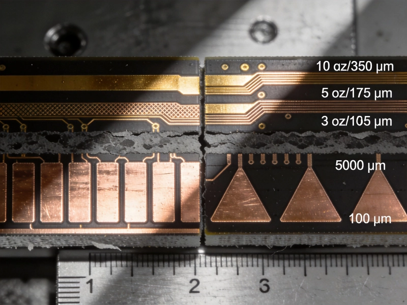
Specify appropriate board thickness and Copper Weight for your mechanical requirements. Use thermally reinforced pad structures where possible. Avoid excessive thermal cycling during assembly. For extreme cases, consider via-in-pad filled structures or mechanical fasteners instead of relying solely on solder joints for high-current connections.
For mission-critical applications, 100% electrical testing of critical current paths provides valuable quality assurance. For standard commercial applications, statistical process control and regular sample testing typically suffices. Match your testing level to your reliability requirements and failure consequence.
This article is intended for informational purposes. Consult with qualified electronics manufacturing engineers and reliability specialists for specific application requirements.
High Current PCB Material Showdown: FR4 vs. Metal-Core vs. PolyimideJuly/14/2026
Best Material for High Current PCB DesignMay/21/2026
High Current PCB EMI Shielding: Ground Pour vs. Shielding CansAugust/14/2026
High Current PCB Conformal Coating: Protecting Solder Joints Under Thermal StressAugust/06/2026
How Much Current Can a PCB Trace Carry? Complete Engineering GuideMay/20/2026
Best Material for High Current PCB Design: How to Choose the Right SubstrateJune/05/2026
High Current PCB Design for Audio Amplifiers: Avoiding Ground LoopsSeptember/14/2026
Cost Comparison: 2oz vs 4oz Copper PCB — What You Need to KnowJune/26/2026