

Designing a Dc-dc Converter capable of delivering 50 amperes isn't just about selecting the right IC or MOSFETs. The Pcb Layout often determines whether your design will perform reliably or become a thermal disaster waiting to happen. After building several high-current converters, I've accumulated hard-won lessons that aren't always obvious from datasheets alone.
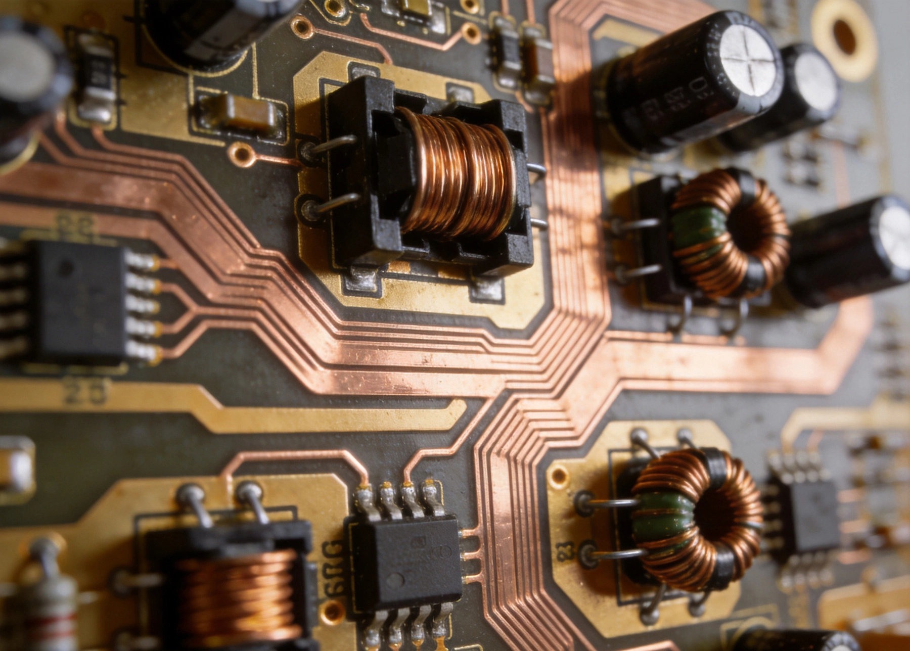
At 50A, even milliohm-level resistances create significant power losses. A trace with just 1mΩ resistance at 50A dissipates 2.5 watts—heat that must go somewhere. Unlike low-current designs where PCB resistance is often negligible, high-current layouts treat copper traces as circuit elements that must be carefully engineered.
The skin effect becomes relevant too. At 50A with switching frequencies in the hundreds of kilohertz, current tends to flow near conductor surfaces, effectively reducing copper cross-section and increasing apparent resistance. Your layout decisions directly impact efficiency, thermal performance, and electromagnetic compatibility.
Standard 1oz copper (about 1.4mil thick) simply won't cut it for 50A continuous operation without excessive temperature rise. For robust designs, use 2oz or even 4oz copper. The relationship between trace width, current, and temperature rise follows predictable curves, but practical experience shows that calculated widths often need to be increased by 50-100% for reliable margin.
For a 50A power path on 2oz copper, you're looking at traces requiring 300-500 mils (7-12mm) width just for the high-current loops. This constraint forces creative routing strategies—sometimes it makes sense to use multiple parallel traces or dedicated bus bars for the heaviest current paths.
Every switching converter has a high-current loop consisting of the input capacitor, power switches, and inductor. In a buck converter, this loop includes the input capacitor, high-side MOSFET, low-side MOSFET (or diode), and the inductor input. Minimizing this loop's area is arguably the single most important layout consideration.
A compact high-current loop reduces:
Place input capacitors directly adjacent to the MOSFETs—ideally within 2mm. Use solid copper pours rather than traces for these paths; the entire area contributes to Current Distribution and reduces effective resistance.
Accurate current sensing is essential for overcurrent protection and current-mode control. If you're using a sense resistor, the voltage sensing leads must connect directly to the resistor pads—not to the adjoining traces carrying load current. This Kelvin Connection prevents voltage drops in the sense path from corrupting your measurement.
The same principle applies to output voltage sense points. Connect directly to the output capacitor or load terminals, not to intermediate traces where Ir Drop occurs. At 50A, even a few milliohms of trace resistance can cause significant voltage error at the load.
Heat must escape the PCB somehow. Thermal Vias placed under power components provide a path from top-layer copper to internal or bottom-layer planes. Use multiple small vias (8-12 mil drill) rather than fewer large ones—they provide better thermal conductivity due to barrel surface area.
For MOSFETs and inductors handling significant dissipation, array Thermal Vias on a 1-1.2mm pitch pattern under the component pad. The vias should connect to a dedicated thermal Copper Pour that's isolated from signal grounds but connected to the main ground plane.
Hot components shouldn't be placed near temperature-sensitive parts. Keep the inductor away from the control IC and feedback traces. The input capacitor, which experiences high RMS current and some dissipation, shouldn't heat the output capacitors or voltage reference components.
Consider airflow direction when placing components. If your application has forced air cooling, position heat-generating components in the airflow path and ensure thermal vias align with natural convection channels.
High-current converters present a classic conflict: you need a solid ground plane for switching noise control, but the high-current return paths create voltage differences across the ground plane that can affect sensitive measurements.
The solution involves a split or hybrid ground approach. Keep the power ground (return path for input capacitors, output capacitors, and switching currents) as a continuous plane. Create a separate signal ground island for the control IC's ground pin, connected to the power ground at a single point—typically near the sense resistor or output capacitor.
This single-point connection prevents high-frequency switching currents from flowing through the signal ground reference, which would otherwise inject noise into the control circuitry. Many successful designs use this approach with great results.
The switching node—the point where the high-side and low-side MOSFETs connect—is simultaneously the noisiest node in the converter and one that requires careful handling. This node swings between input voltage and ground at the switching frequency, creating dv/dt edges that couple to nearby traces.
Keep the switching node area as small as possible while maintaining adequate clearance for the required voltage rating. Route it away from sensitive traces, especially the feedback voltage sense line and any analog signals. If possible, shield the switching node with ground copper on adjacent layers.
The feedback path from output to control IC determines regulation accuracy. Even small noise injection here causes jitter in the output voltage, which manifests as increased ripple or spurious spectral components. Route feedback traces as short as possible, away from highdv/dt nodes like the switching node and high-current paths.
Some designs benefit from using a RC filter on the feedback trace right at the IC input. This dampens any high-frequency noise that manages to couple onto the sense line. Values in the range of 10Ω in series with 1nF to ground often work well, but check your specific IC's recommendations.
Beyond theory, real-world builds teach lessons that simulations miss. First, always build and test with a current probe before committing to final layout. Probe the input current waveform, switching node, and output ripple—you'll catch problems early when modifications are easy.
Second, include test points for critical measurements. Add Kelvin-connected test points for input voltage, output voltage, and current sense resistor voltage. You'll thank yourself when debugging thermal issues or optimizing efficiency.
Third, consider manufacturing realities. Traces narrower than 8-10 mils with 2oz copper are difficult to manufacture consistently. Leave adequate clearance around high-voltage nodes for your specific manufacturer's capabilities. Production boards often behave differently than prototypes due to variations in solder paste deposition and reflow profiles.
Several mistakes appear repeatedly in 50A converter designs. The first is insufficient input capacitance. At 50A, input ripple current is substantial. Use multiple capacitors in parallel—ceramic for high-frequency response, bulk electrolytic or polymer for energy storage. One or two small caps simply won't handle the RMS current requirements.
Another common error is inadequate clearance between high-voltage and low-voltage circuits. In converters with high input voltages, creepage and clearance requirements can force surprising layout constraints. Plan for safety spacing from the beginning, not as an afterthought.
Finally, don't underestimate the importance of the inductor. The inductor choice affects more than just inductance value—physical size, saturation current rating, and DC resistance all impact thermal performance. A borderline inductor at room temperature may fail catastrophically at elevated ambient temperatures.
Building a reliable 50A Dc-dc Converter requires treating the PCB as a critical circuit element, not just mechanical support. The high-current loop demands minimal area. Thermal Management requires proactive planning with appropriate copper weights, thermal vias, and Component Placement. Grounding strategy separates power and signal domains at a single controlled point.
Successful designs balance competing requirements: minimal loop area versus manufacturing constraints, thermal performance versus component density, and EMI performance versus layout complexity. Each project involves tradeoffs, but understanding these principles helps you make informed decisions rather than lucky guesses.
Start with conservative margins in your first revision. You can always optimize later once the baseline design works reliably. But debugging thermal problems or EMI failures consumes far more time than building in adequate margins initially. Let your first prototype teach you what the simulations couldn't.
What's the minimum Copper Weight for a 50A converter?
For reliable operation without excessive temperature rise, 2oz copper is the minimum recommendation. Use 3oz or 4oz for the most demanding applications or constrained layouts.
How close should input capacitors be to the MOSFETs?
Keep the distance under 2mm for optimal performance. Any extra distance adds series inductance that creates voltage spikes and increases EMI.
Can I use planes for all high-current traces?
Planes are generally better than traces for high-current paths due to lower resistance and better Current Distribution. However, ensure proper thermal relief connections if the plane needs to connect to smaller pads.
How do I reduce EMI from the switching node?
Minimize switching node area, use ground shielding on adjacent layers, slow down the switching edges (if your IC allows adjustment), and filter the feedback path.
Should power ground and signal ground be connected?
Yes, but at a single point to prevent switching currents from flowing through the signal reference. Connect them near the current sense point or output capacitor.
Building a High Current PCB Power Supply for Server RacksJuly/30/2026
Copper Pour vs Trace: What 3 Years of PCB Failures Taught UsMay/21/2026
High Current PCB Daisy-Chain vs. Star Routing: Voltage Drop ComparisonAugust/08/2026
High Current PCB vs. Standard PCB: A Real-World Thermal Stress TestJuly/09/2026
Heavy Copper vs Standard Copper PCB: Complete Comparison Guide for EngineersMay/20/2026
High Current PCB Design for Uninterruptible Power Supplies (UPS)September/02/2026
High Current PCB Current Crowding: Sharp Corners vs. Teardrop TransitionsSeptember/03/2026
5 Critical Thermal Management Problems in High Power PCBsMay/21/2026