

Why smart engineers stopped using trace width calculators—and started understanding the physics
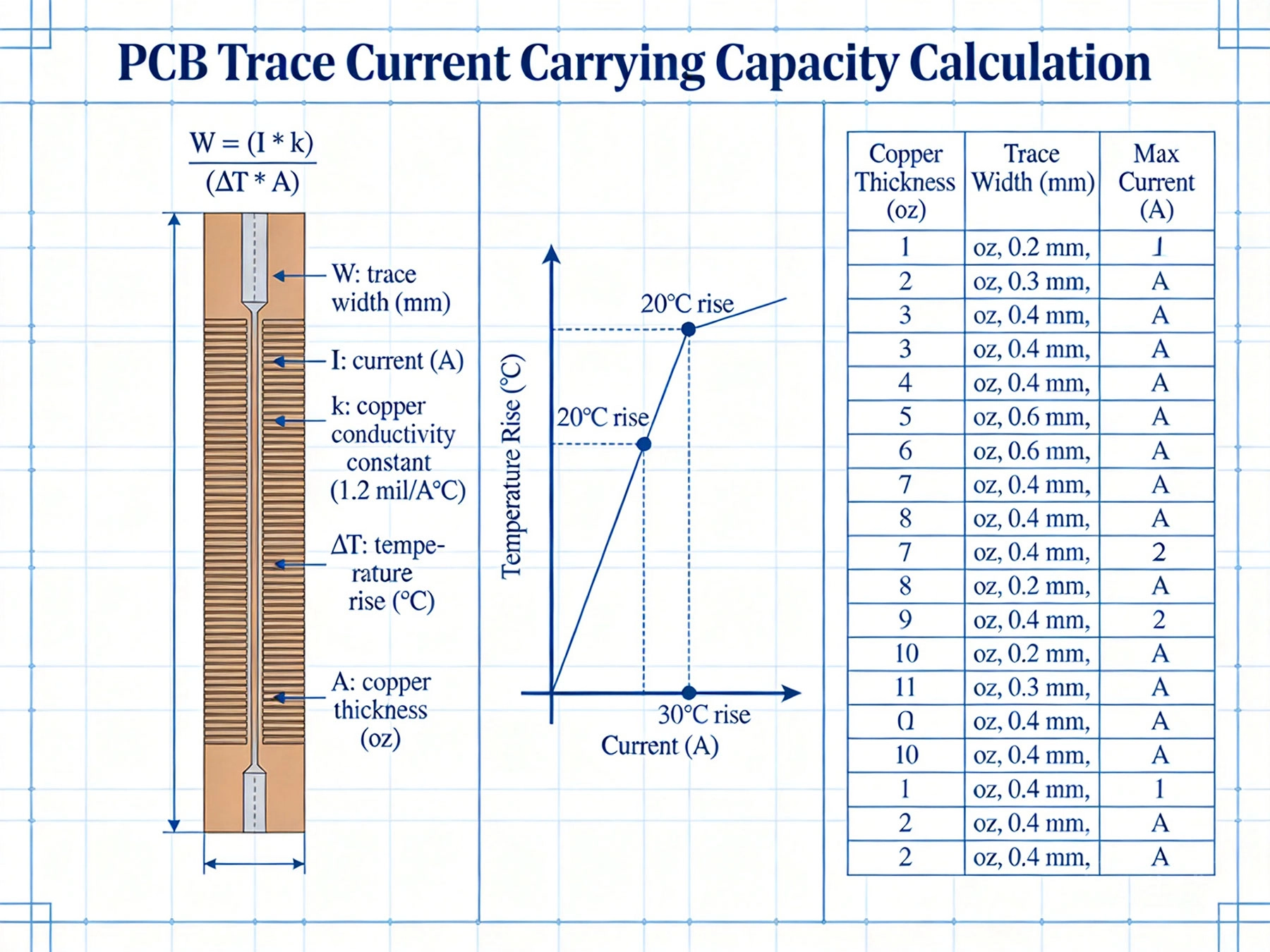
Why Ipc-2152 Changes Everything
For decades, PCB designers relied on Ipc-2221 (formerly MIL-STD-275) trace width charts. The problem? Those charts were derived empirically in the 1950s using boards and materials that bear little resemblance to modern PCBs.
Ipc-2152, released in 2009, takes a fundamentally different approach. Instead of lookup tables, it provides a physics-based model that accounts for:
| Factor | Ipc-2221 (1950s) | IPC-2152 (Modern) |
|---|---|---|
| Basis | Empirical measurements | Physics-based thermal modeling |
| Board types | Single-sided, simple | Multilayer, complex stackups |
| Copper weights | Limited to standard weights | Any Copper Thickness |
| Accuracy | Conservative (often overly) | Tunable based on conditions |
| Space efficiency | Wastes board area | Optimized for real conditions |
At its core, IPC-2152 balances heat generation against Heat Dissipation. The trace heats up due to resistive losses (I²R), and cools down through conduction, convection, and radiation.
But here's where it gets interesting. The k factor accounts for your specific conditions:
| Condition | k Value | Impact |
|---|---|---|
| External trace, still air | 0.024 | Baseline condition |
| External trace, forced air | 0.048 | 2× current capacity |
| Internal trace | 0.024 × 0.5 | ~30% less capacity |
| Trace on polyimide | 0.020 | Slightly reduced |
Requirements:
Use these as starting points, then verify with calculations for your specific conditions.
Choosing ΔT is the most consequential decision. Common guidelines:
IPC-2152 uses "base copper" thickness. But finished traces include plating:
| Nominal | Base Cu | After Plating | Effective |
|---|---|---|---|
| 1 oz | 0.7 mil | +0.8 mil plating | ~1.5 oz |
| 2 oz | 1.4 mil | +0.8 mil plating | ~2.3 oz |
For precision calculations, confirm actual finished trace thickness with your PCB manufacturer.
Internal (buried) traces have significantly reduced current capacity because:
Rule of thumb: Internal traces need 2× the width of external traces for the same current.
When traces connect to large copper planes:
In multilayer designs:
Never trust calculations alone:
Most online "trace width calculators" use simplified IPC-2221 formulas. Here's what they get wrong:
| Calculator Issue | Reality |
|---|---|
| Assumes 1 oz copper only | IPC-2152 works for any thickness |
| Fixed ambient temperature | Should match your environment |
| Ignores airflow | Forced air doubles capacity |
| No internal trace adjustment | Internal traces need 2× width |
| Conservative "safety factor" | Often wastes 50%+ board space |
IPC-2152 gives you the tools to design Pcb Traces that are both safe and space-efficient. The key is understanding your actual operating conditions—not just plugging numbers into a calculator.
Remember:
Master these principles, and you'll never wonder "is this trace wide enough?" again.
Want to run your own IPC-2152 calculations? Search for "IPC-2152 calculator spreadsheet" or check your EDA tool—modern versions of Altium, Cadence, and KiCad include IPC-2152-based trace width calculators in their constraint managers.
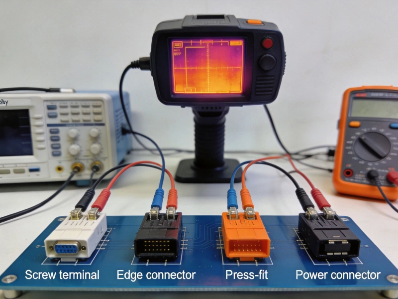
High Current PCB Connector Selection: Test Results and Real Performance DataMay/21/2026
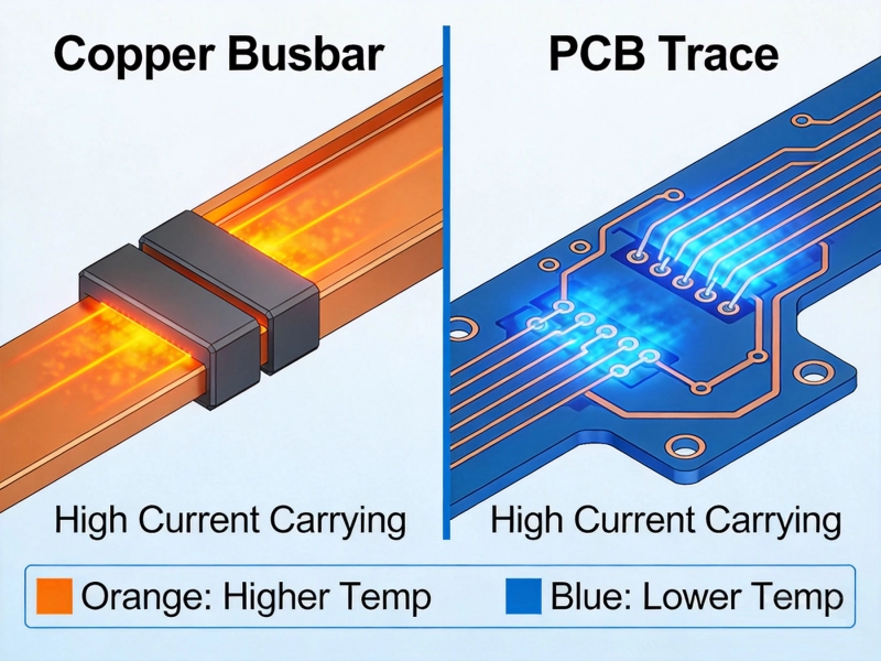
Bus Bar vs PCB Trace for High CurrentMay/21/2026
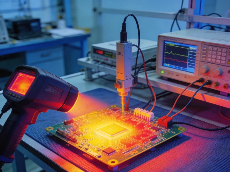
High Current PCB Testing: Thermal Imaging vs. 4-Wire Kelvin MeasurementJuly/22/2026
High Current PCB Bus Bars vs. Heavy Copper Traces: Cost and PerformanceJuly/25/2026
High Current PCB Annular Rings: Minimum Size vs. Reinforced SizeAugust/12/2026
High Current PCB Via Plating: 1mil vs. 2mil Thickness Reliability TestAugust/03/2026
High Current PCB Current Crowding: Sharp Corners vs. Teardrop TransitionsSeptember/03/2026
Designing a High Current PCB Motor Driver: Avoiding EMI PitfallsJuly/14/2026