
Designing Printed Circuit Boards (PCBs) for high-current applications requires a distinct approach compared to standard signal-level designs. Whether you are building power supplies, motor controllers, or battery management systems, managing heat and preventing voltage drops are paramount. Failure to adhere to High Current Pcb Design guidelines can result in catastrophic failures, including delamination, trace burning, or fire.
This article outlines the critical factors engineers must consider when routing high currents on a PCB.
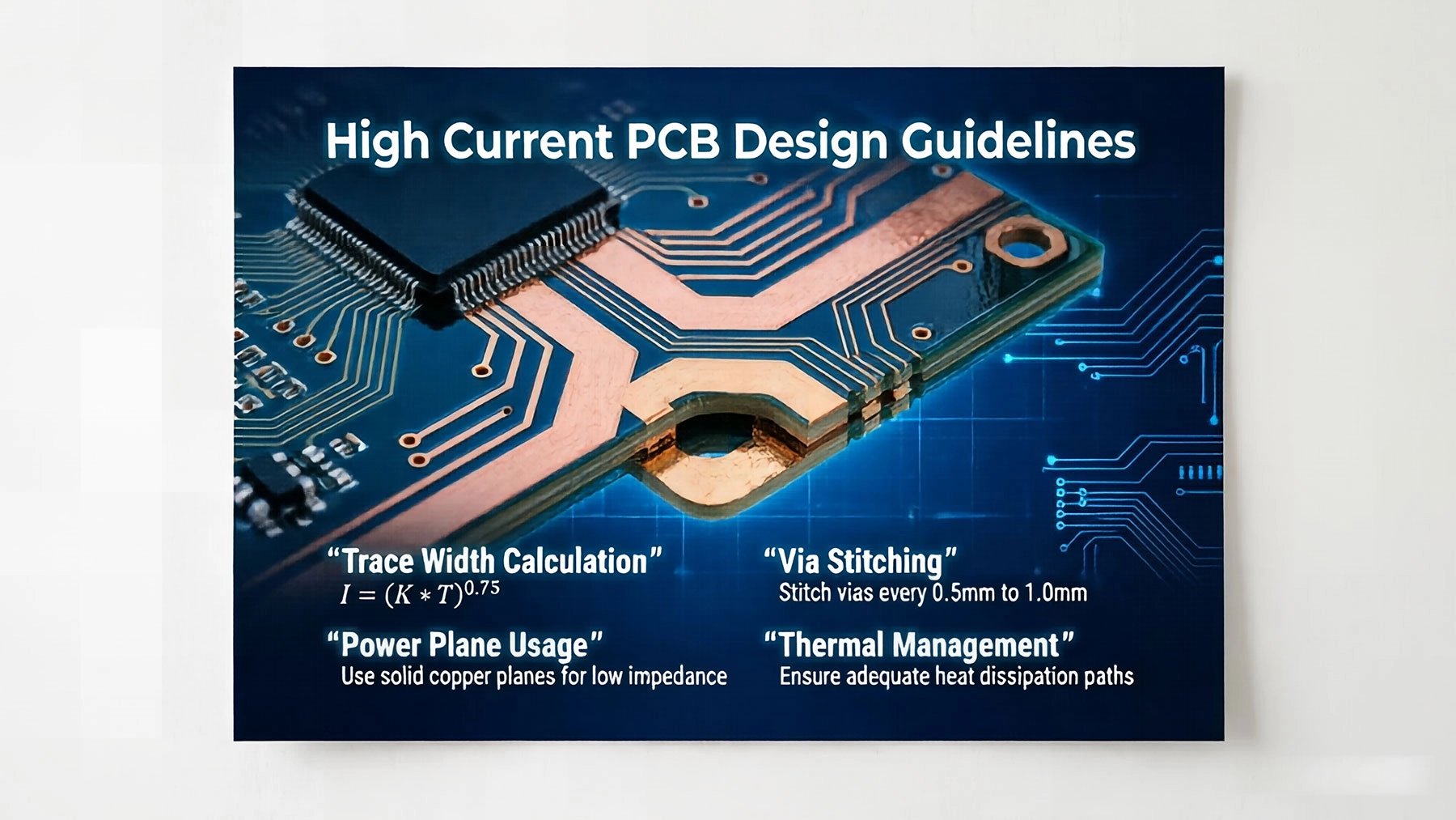
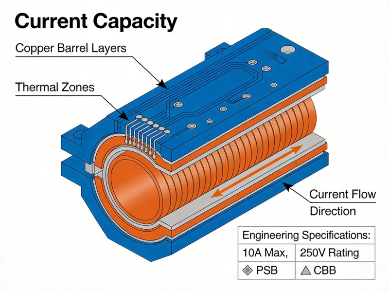
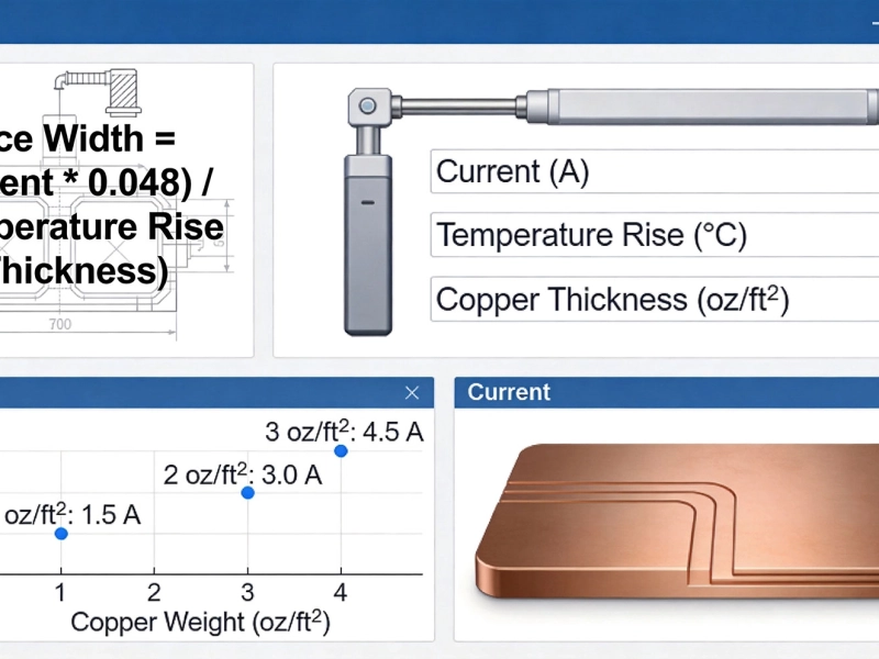
The most fundamental rule of high-current design is ensuring the copper trace is wide and thick enough to handle the amperage without overheating.
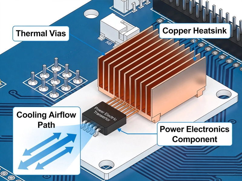
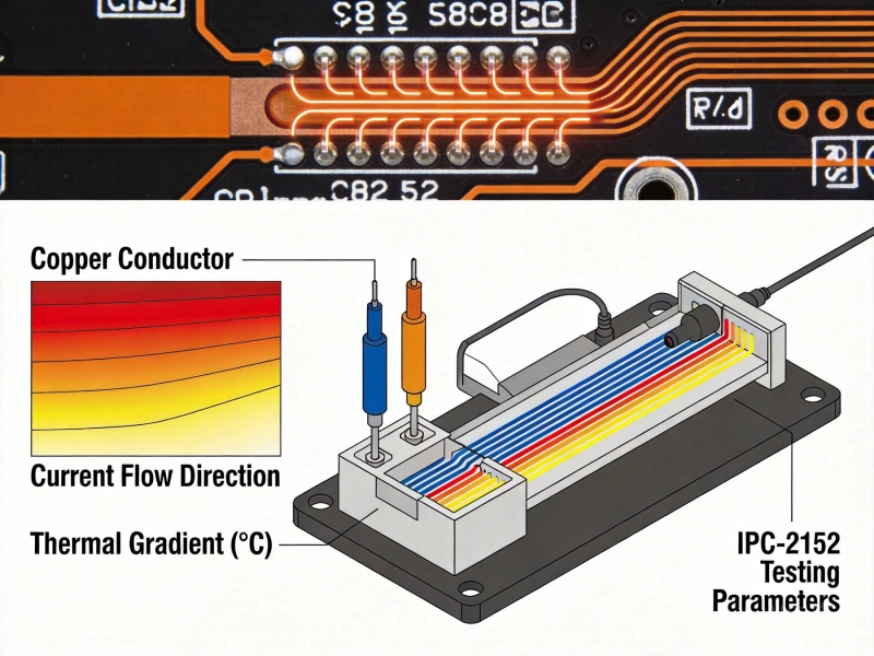
High Current generates significant heat ($I^2R$ losses). If this heat isn't dissipated, the PCB temperature will rise, potentially damaging components or the board substrate itself.
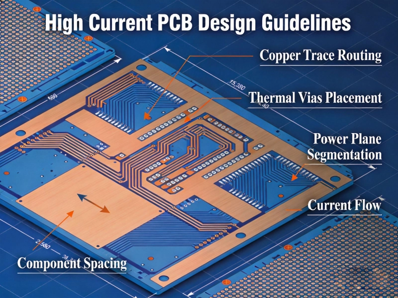
How you route the traces matters just as much as their physical dimensions.
The components themselves must be rated for the thermal environment created by high currents.
Successful High Current Pcb Design is a balancing act between electrical performance, Thermal Management, and manufacturability. By strictly following IPC standards, optimizing Copper Weight, and employing smart layout techniques, engineers can create robust boards capable of handling demanding power loads safely.
Why Your High-Power PCBs Overheat (And the 5 Methods That Actually Fix It)May/20/2026
Plated Through Hole Current Rating: Complete Guide for PCB DesignersMay/21/2026
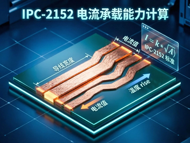
Mastering IPC-2152 Current Carrying Capacity Calculation for Reliable PCB DesignJune/04/2026

5 Critical Thermal Management Problems in High Power PCBsMay/21/2026
High Current PCB Trace Width Calculator: The Ultimate Engineering GuideMay/20/2026
IPC-2152 Current Carrying Capacity Calculation GuideJune/03/2026
High Current PCB Design GuidelinesMay/21/2026
Best Material for High Current PCB Design: How to Choose the Right SubstrateJune/05/2026