

High Current PCB routing requires careful attention to Trace Geometry, Thermal Management, and electromagnetic compatibility. Among the many decisions designers face, the choice between 45-degree angled traces and curved traces often sparks debate. While both approaches can deliver functional designs, they offer distinct advantages and trade-offs that impact electrical performance, manufacturability, and electromagnetic behavior. This comprehensive analysis examines these two routing styles from practical, technical, and manufacturing perspectives to help you make informed decisions for your High Current PCB designs.
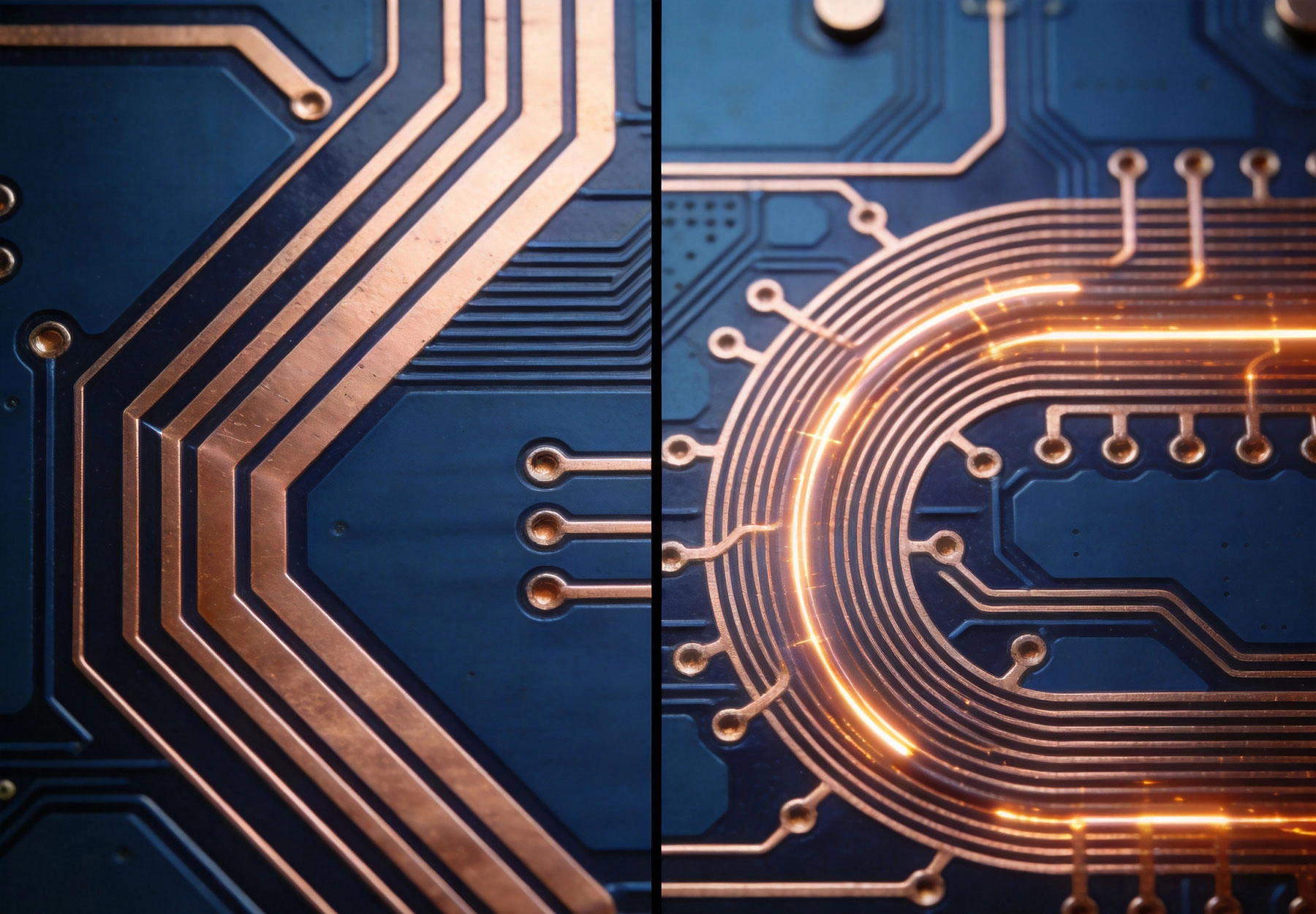
Before diving into the specific comparison of routing styles, it's essential to understand the unique challenges that High Current Pcb routing presents. When currents exceed a few amps, conventional Pcb Design rules no longer suffice, and specialized techniques become necessary.
High Current traces must handle substantial current without excessive heating. Current Density, measured in amps per square millimeter of copper cross-section, determines how much current a trace can safely carry. Excessive Current Density leads to resistive heating, which can damage the PCB substrate, compromise solder joints, and potentially create fire hazards.
The relationship between current, trace width, and temperature rise follows established guidelines like Ipc-2152. For a given Copper Thickness, wider traces can carry more current with lower temperature rise. However, board space is always limited, creating tension between current capacity and physical constraints.
Heat generation in copper traces follows the formula P = I²R, meaning power dissipation increases with the square of current. A trace carrying 20 amps generates four times the heat of an equivalent trace carrying 10 amps. This heat must be effectively dissipated to prevent temperature rise beyond safe limits.
Trace Geometry affects both heat generation and Heat Dissipation. The electrical resistance of a trace depends on its length and cross-sectional area. Wider traces have lower resistance and generate less heat for a given current. Additionally, the surface area of a trace affects its ability to dissipate heat to the surrounding air and PCB substrate.
High Current traces create stronger magnetic fields than signal traces, increasing electromagnetic compatibility concerns. Sudden changes in trace direction can create discontinuities in current flow, leading to inductive spikes and electromagnetic interference. The geometry of trace corners and transitions becomes particularly important when dealing with high currents and fast switching edges.
45-degree routing has been the standard in Pcb Design for decades. This approach uses straight line segments connected at 45-degree angles to create paths that approximate curves while maintaining the precision and predictability of straight traces.
The dominance of 45-degree routing stems from early Pcb Manufacturing limitations. Traditional photoplotters and early CAD systems were optimized for orthogonal and 45-degree geometries. While modern manufacturing and design tools have largely overcome these constraints, 45-degree routing remains deeply embedded in PCB design culture and continues to offer practical advantages.
Many experienced PCB designers default to 45-degree routing out of habit and familiarity. Design review processes, design rule checking, and manufacturing specifications are often built around this convention. Deviating from the standard requires justification and may raise questions during review processes.
From an electrical perspective, 45-degree corners represent a reasonable compromise between routing efficiency and electrical performance. The corner maintains consistent trace width through the bend, avoiding the narrowing that occurs in 90-degree corners. This consistency helps maintain uniform current density and prevents localized heating at corners.
For most high current applications below several tens of amps, 45-degree corners provide adequate performance. The inductive discontinuity introduced by a 45-degree bend is minimal compared to the overall trace inductance, and the radiated electromagnetic energy is generally within acceptable limits.
Manufacturing processes are well-optimized for 45-degree geometries. Photolithography, etching, and inspection systems handle these angles reliably. The straight-line segments of 45-degree routing align well with the pixel-based nature of imaging systems and the grid-based approach of many manufacturing processes.
Design rule checking is straightforward with 45-degree routing. Minimum trace widths and spacings can be verified using simple geometric calculations. Manufacturing variations affect 45-degree traces predictably, making it easier to ensure design robustness.
In many cases, 45-degree routing provides the most space-efficient path between two points. The ability to make diagonal connections can reduce overall trace length compared to purely orthogonal routing. This efficiency is particularly valuable in high current designs where wide traces consume significant board area.
For designs with dense Component Placement and multiple high current paths, 45-degree routing often enables more compact layouts than curved traces, which may require additional clearance for their sweeping arcs.
Despite its advantages, 45-degree routing has limitations in high current applications. Each corner represents a discontinuity in the current path, creating localized electromagnetic field concentrations. At very high currents or fast switching frequencies, these discontinuities can generate significant electromagnetic interference.
The sharp transitions at 45-degree corners can create stress concentrations in the copper, potentially affecting reliability under Thermal Cycling. While modern PCB materials and manufacturing processes minimize this concern, it remains a consideration for extreme reliability requirements.
Curved trace routing, once rare due to manufacturing constraints, has become increasingly common with modern PCB design tools and fabrication capabilities. Smooth curves offer theoretical electrical advantages that make them attractive for high current and high frequency applications.
The primary theoretical advantage of curved traces is the elimination of sharp discontinuities in the current path. A smooth curve provides constant trace width and gradual direction changes, minimizing the inductive spikes and electromagnetic field concentrations that occur at sharp corners.
For high frequency signals or fast-switching high current paths, curved traces can reduce electromagnetic interference and improve signal integrity. The continuous nature of curves eliminates the reflection points created by angled corners, potentially improving performance in sensitive applications.
In high current DC applications, curved traces distribute current more uniformly through bends, avoiding the Current Crowding that can occur at the inside corner of angled traces. This uniform distribution can reduce localized heating and improve overall Current Carrying Capacity.
The uniform cross-section of curved traces provides consistent thermal performance through bends. Unlike angled corners where thermal hot spots can develop at the inside corner, curved traces maintain more even temperature distribution.
For applications where Thermal Management is critical, curved traces may offer marginal improvements in Heat Dissipation. The increased surface area of a curved path compared to an equivalent angled path can provide slightly better heat transfer to the surrounding environment.
Beyond technical considerations, curved traces offer aesthetic advantages. A board with flowing curved traces often appears more refined and professional than one with angular routing. For consumer-facing products or applications where visual impression matters, curved routing can enhance perceived quality.
This aesthetic consideration, while seemingly minor, can influence design reviews and product presentations. A well-crafted curved layout demonstrates attention to detail and design craftsmanship that may positively influence stakeholders.
Contemporary PCB design software makes curved routing as easy as traditional 45-degree routing. Interactive routing tools support real-time curve creation and modification. Design rule checking has evolved to handle curved geometries accurately. These capabilities remove the historical barriers that made curved routing impractical.
Advanced routing algorithms can optimize curved paths for length, clearance, and manufacturability. Some tools offer automated conversion between routing styles, allowing designers to experiment with both approaches during the design process.
Despite their advantages, curved traces present practical challenges. The mathematical complexity of curves complicates design rule checking and manufacturing verification. While modern systems handle these complexities well, the underlying complexity remains.
Curved traces generally consume more board area than equivalent 45-degree routing for the same path. The sweeping arcs required for smooth curves need additional clearance, potentially reducing routing density in space-constrained designs.
Manufacturing process optimization has historically focused on orthogonal and 45-degree geometries. While modern processes handle curves effectively, some legacy equipment and processes may still perform better with traditional angles.
Electromagnetic compatibility represents one of the most significant differentiators between routing styles in high current applications. Understanding these effects helps designers make appropriate choices for their specific requirements.
At sharp corners, current tends to concentrate at the inside edge of the turn. This Current Crowding increases current density locally, leading to higher resistive losses and localized heating. For high current traces, this effect can create measurable hot spots at corners.
45-degree corners mitigate but do not eliminate this effect. The change in direction is less abrupt than 90-degree corners, reducing but not eliminating current crowding. Curved corners distribute current most uniformly, minimizing hot spots and providing the most consistent electrical performance.
Current flowing through a conductor generates a magnetic field that circles the conductor according to the right-hand rule. At corners, the geometry of this field becomes complex, with field lines concentrating at the outside of the turn.
Sharp corners create more concentrated magnetic fields than gradual curves. This concentration can increase electromagnetic interference with adjacent traces and components. For high current traces in sensitive analog circuits or near communication lines, this interference can cause significant performance degradation.
Fast-switching high current paths are significant sources of radiated electromagnetic energy. The frequency content of switching edges determines the wavelength of radiated energy, with higher frequencies having shorter wavelengths and different radiation characteristics.
For switching frequencies above several hundred kilohertz, the wavelength becomes comparable to typical Pcb Trace lengths, making trace geometry increasingly important for electromagnetic compatibility. Curved traces generally produce lower radiated emissions than equivalent angled traces due to their smoother current transitions.
However, for purely DC or low-frequency high current applications (such as battery distribution or motor power), these high-frequency effects are negligible, and the choice between routing styles has minimal electromagnetic compatibility impact.
The practical realities of Pcb Manufacturing influence routing decisions. Understanding how different trace geometries interact with fabrication processes helps designers create manufacturable, reliable, and cost-effective high current PCBs.
Chemical etching removes unwanted copper to create the desired trace pattern. The etching process affects different geometries in characteristic ways. Undercutting, where etchant attacks the sides of traces, tends to be more pronounced at sharp corners than along straight segments or gentle curves.
45-degree corners experience more undercutting than curved corners due to the concentration of etching at the corner point. This undercutting can reduce the effective trace width at corners, potentially creating weak points in high current paths. However, modern controlled-etch processes minimize these effects for both routing styles.
Curved traces, with their uniform geometry, experience more consistent etching along their length. This consistency can result in more predictable electrical performance, particularly for precision high current applications.
The imaging process transfers the design pattern to the photoresist layer on the copper-clad board. Digital imaging systems use pixels to represent trace geometry, creating a fundamental relationship between trace geometry and imaging resolution.
45-degree traces align well with the square pixels of imaging systems, creating clean diagonal lines with minimal pixelation artifacts. Curved traces require more pixels to represent accurately, and may show slight faceting at the resolution limits of the imaging system.
For high-resolution imaging systems (typically 1 mil or finer pixel size), these effects are negligible for both routing styles. However, lower resolution systems may produce better results with 45-degree geometry due to its alignment with the pixel grid.
Automated optical inspection (AOI) systems verify that manufactured boards match design specifications. These systems compare captured images against design data, checking for defects including trace width violations, shorts, and opens.
45-degree geometry simplifies AOI algorithms, as the straight-line segments and known angles create predictable patterns for defect detection. Curved geometry requires more sophisticated image processing but is well within the capabilities of modern AOI systems.
For critical high current applications, additional inspection including cross-section analysis may verify Copper Thickness and integrity at corners and transitions. Both routing styles can be effectively inspected using standard techniques.
Based on the technical analysis and practical considerations, specific guidelines emerge for selecting between 45-degree and curved routing in High Current Pcb designs.
Space-Constrained Designs: When board area is limited and every millimeter counts, 45-degree routing often provides the most compact solution. The ability to make diagonal connections can reduce overall trace length and required board area.
High Density Layouts: In designs with multiple high current paths or dense Component Placement, the space efficiency of 45-degree routing may be essential for achieving a manufacturable layout.
Legacy Compatibility: When working with existing design standards, manufacturing specifications, or design review processes built around 45-degree conventions, maintaining consistency may outweigh the benefits of curved routing.
Low to Moderate Currents: For currents below 20 amps where electromagnetic effects are minimal and thermal considerations are manageable, 45-degree routing provides adequate performance with maximum design efficiency.
Cost-Sensitive Applications: When manufacturing costs must be minimized and the application can tolerate the minor compromises of 45-degree routing, this traditional approach offers proven reliability at competitive cost.
High Frequency Switching: For switching power supplies, motor drives, and other applications with fast current transitions, curved routing minimizes electromagnetic interference and inductive effects that can cause noise and reliability issues.
Very High Currents: When currents exceed 30-50 amps, the benefits of uniform Current Distribution and minimized hot spots at corners become increasingly significant. Curved routing helps manage the extreme thermal and electromagnetic challenges of very high current designs.
EMC-Critical Applications: In designs with strict electromagnetic compatibility requirements, such as medical equipment, aerospace systems, or products with sensitive analog circuits, curved routing can provide measurable improvements in noise performance.
Aesthetic Requirements: For consumer products where visual presentation matters, or professional equipment where design quality reflects brand image, curved routing creates a more refined appearance.
Ample Board Space: When board area is not constrained, curved routing allows optimization for electrical performance without compromising layout density.
Many effective designs use a combination of routing styles, applying each where it provides the greatest advantage. Critical high current paths may use curved routing for optimal electrical performance, while less critical connections use 45-degree routing for space efficiency.
This hybrid approach requires careful attention to transitions between routing styles. A curved trace should transition smoothly to straight segments rather than creating abrupt changes in curvature. Proper transition design maintains the electrical benefits of curved routing while achieving layout efficiency where needed.
Regardless of routing style choice, certain best practices apply to all high current PCB designs.
Trace width should remain constant through corners and transitions. Tapering traces at corners, sometimes proposed to match Current Distribution, actually creates additional discontinuities and should be avoided. The trace should maintain its full design width throughout any direction changes.
Even when using 45-degree routing, avoid 90-degree corners where possible. If 90-degree turns are unavoidable, consider using two 45-degree corners with a short straight segment between them, effectively creating a chamfered corner that reduces current crowding.
High current traces generate stronger electromagnetic fields than signal traces and require greater spacing from sensitive circuits. Maintain adequate clearance between high current paths and analog, RF, or communication circuits regardless of routing style.
Trace geometry and Copper Weight interact to determine Current Carrying Capacity. Thicker copper allows narrower traces for equivalent current, but manufacturing constraints may limit minimum trace widths and spacing. Optimize both Copper Weight and trace geometry for the specific application requirements.
High current traces generate heat that must be managed. Consider Thermal Vias to spread heat to internal copper planes, copper pours to increase heat dissipation area, and proximity to Heat Sinks or cooling airflow. The routing style should support rather than compromise thermal management strategies.
Examining specific applications helps illustrate the practical considerations that influence routing style selection.
A 500-watt switching power supply operating at 100 kHz presents challenging routing requirements. The switching node carries high currents with fast transitions, creating significant electromagnetic interference potential.
In this application, curved routing for the switching node minimizes inductive spikes and reduces radiated emissions. The input and output power paths, carrying DC current with minimal switching content, use 45-degree routing for space efficiency. This hybrid approach optimizes both electromagnetic performance and board area utilization.
Battery management systems for electric vehicles distribute currents of 50-200 amps across multiple cells and modules. The high currents and reliability requirements make trace geometry critical.
Curved routing for main Power Distribution paths provides uniform current distribution and minimizes hot spots. The gradual curves handle thermal expansion stresses better than sharp corners, improving reliability in the automotive temperature range. Less critical signal traces use conventional 45-degree routing.
A variable frequency drive for a 20-horsepower industrial motor switches currents of 30-40 amps at carrier frequencies of 4-8 kHz. The combination of high current and switching frequency creates demanding electromagnetic compatibility requirements.
Curved routing for the inverter output stage reduces electromagnetic interference that could affect motor bearings and nearby equipment. The input rectifier stage, operating at lower frequency, uses 45-degree routing. Design validation through electromagnetic compatibility testing confirms the effectiveness of this approach.
Evolving technologies and design practices continue to influence High Current Pcb Routing approaches.
Improvements in imaging resolution, etching control, and inspection technology reduce the manufacturing advantages historically enjoyed by 45-degree routing. As these capabilities continue to advance, curved routing becomes increasingly practical for all applications.
Electromagnetic simulation tools enable designers to analyze the effects of trace geometry on current distribution, thermal performance, and electromagnetic compatibility. These tools help optimize routing decisions based on quantitative analysis rather than rules of thumb.
Electric vehicles, renewable energy systems, and high-power computing continue to push current requirements higher. As currents increase, the benefits of optimized trace geometry become more significant, favoring approaches that minimize discontinuities and current crowding.
The choice between 45-degree angled traces and curved traces in High Current Pcb Routing is not a matter of one being universally superior. Each approach offers distinct advantages that make it appropriate for specific applications.
45-degree routing provides proven, efficient solutions for space-constrained designs and moderate current applications. Its compatibility with established manufacturing processes and design conventions makes it a reliable choice for many projects. The space efficiency and manufacturing simplicity of 45-degree routing ensure its continued relevance in PCB design.
Curved routing offers superior electrical performance for demanding applications with high currents, fast switching, or strict electromagnetic compatibility requirements. The uniform current distribution and minimized discontinuities of curved traces provide measurable benefits in challenging designs. As manufacturing capabilities and design tools continue to evolve, curved routing becomes increasingly practical for a broader range of applications.
The most effective approach often combines both routing styles, using each where it provides the greatest advantage. Critical high current paths benefit from curved geometry, while less demanding connections use 45-degree routing for efficiency. This hybrid approach requires careful design to ensure smooth transitions and consistent performance.
Regardless of routing style, attention to fundamental High Current Design principles remains essential. Adequate trace width, proper thermal management, and electromagnetic compatibility considerations matter more than the specific geometry of trace corners. By understanding the trade-offs between routing styles and applying appropriate design practices, engineers can create high current PCBs that deliver reliable performance in demanding applications.
For most applications below 20 amps with moderate switching frequencies, the difference is minimal. Curved routing provides measurable benefits for high currents (above 30 amps), fast switching applications, or designs with strict electromagnetic compatibility requirements. The improvement is most significant in the most demanding applications.
Modern manufacturing processes handle curved routing with minimal cost impact for most designs. Very high volume production or specialized applications may see slight cost differences, but for typical quantities, manufacturing costs are comparable between routing styles.
Yes, hybrid approaches are common and effective. Use curved routing for critical high current paths and 45-degree routing for less critical connections. Ensure smooth transitions between routing styles to maintain electrical performance benefits.
Trace width depends on current level, copper thickness, acceptable temperature rise, and cooling conditions. Use Ipc-2152 guidelines or online calculators to determine appropriate widths. As a rough guide, allow 1 mm of trace width per amp for 1oz copper with moderate cooling, scaling proportionally for different copper weights.
90-degree corners should generally be avoided in high current applications due to current crowding and electromagnetic field concentration. If unavoidable, maintain generous trace width at the corner and consider using chamfered corners (two 45-degree corners with a short straight segment) to reduce the severity of the transition.
High Current PCB Snubber Circuits: Placement Impact on Voltage SpikesAugust/06/2026
High Current PCB Heat Sinks: Thermal Pads vs. Direct Copper ExposureAugust/10/2026
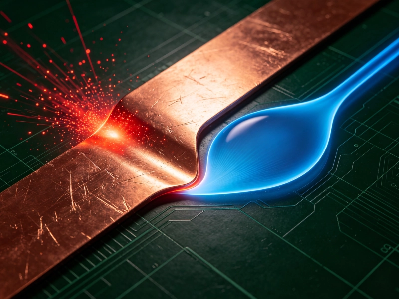
High Current PCB Current Crowding: Sharp Corners vs. Teardrop TransitionsSeptember/03/2026
High Current PCB Pad Design: Reinforced Plating vs. Standard PadsJuly/28/2026
A Deep Dive into High Current PCB Design for Solar InvertersJuly/17/2026
High Current PCB Design GuidelinesMay/21/2026
High Current PCB Failure Modes and PreventionJune/18/2026
Copper Pour vs Trace: What 3 Years of PCB Failures Taught UsMay/21/2026