Every engineer who has designed Power Electronics knows the feeling: you prototype your circuit, power it up, and the temperature climbs beyond specifications. Thermal Management is one of the most critical challenges in power Pcb Design, yet it's frequently addressed through trial and error rather than systematic engineering approaches. Excessive temperature rise compromises component reliability, reduces system efficiency, and can lead to catastrophic field failures.
Power PCB Thermal Management isn't just about adding bigger heat sinks—it's about understanding heat generation, conduction paths, and dissipation methods at the PCB level. By implementing proven thermal design techniques, you can achieve dramatic temperature reduction without increasing board size or cost significantly.

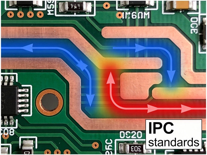
Understanding Heat Generation and Transfer
Before implementing solutions, understand where heat originates and how it moves:
Primary Heat Sources
In power PCBs, heat generation occurs primarily through:
- Conduction losses: I²R losses in MOSFETs, diodes, and other power semiconductor devices
- Switching losses: Energy dissipated during device turn-on and turn-off transitions
- Copper losses: Resistive heating in Pcb Traces carrying high currents
- Passive component losses: Resistors, inductors, and capacitors dissipating energy as heat
Heat Transfer Mechanisms
Heat moves from sources through three mechanisms:
- Conduction: Heat transfer through solid materials—copper planes, vias, and PCB dielectrics
- Convection: Heat transfer to air (natural or forced convection)
- Radiation: Electromagnetic heat transfer, typically a secondary contributor at PCB temperatures
Effective thermal management optimizes each mechanism, creating clear paths for heat to move from sources to ambient without creating hot spots.
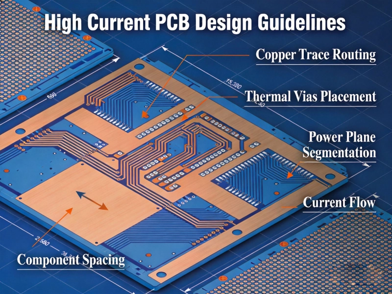
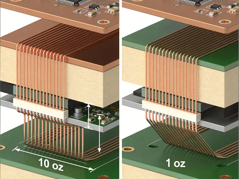
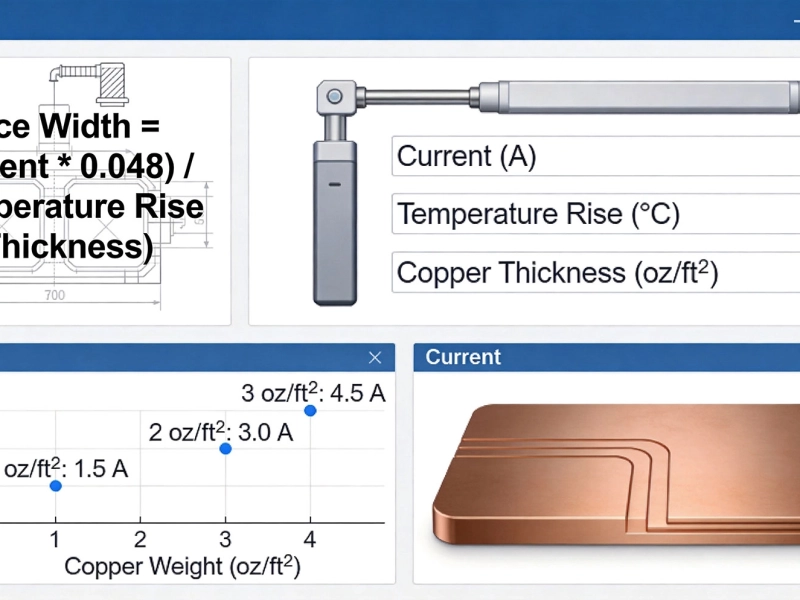
Copper Weight Optimization
The Role of Copper Weight
Copper is your primary thermal conductor in power PCBs:
- Thermal conductivity: Copper conducts heat ~400× better than FR-4 dielectric
- Current Carrying Capacity: Heavier copper reduces resistive heating in traces
- Thermal mass: Heavier copper provides more thermal mass, reducing temperature spikes
Strategic Copper Weight Selection
Apply heavier copper where it matters most:
- Power input sections: Use 2-6oz copper where High Current enters the board
- Power output sections: Heavy copper where current exits to loads
- Component pads: Increase copper under power semiconductor pads (copper pours, thermal reliefs)
- Ground planes: Use full ground planes in 2oz+ copper for heat spreading
- Control signal traces: Standard 1oz copper adequate for low-current control paths
Copper Pour Guidelines
Maximize copper coverage:
- Pour unused areas: Fill all unused board area with copper tied to ground or power planes
- Minimize thermal reliefs: Use solid connections for thermal paths; thermal reliefs only where soldering requires them
- Pad enlargement: Increase pad sizes for power components beyond minimums
- Copper stacking: Align copper across layers to maximize thermal conduction through the board thickness
Thermal Via Arrays
The Power of Thermal Vias
Thermal Vias dramatically improve heat transfer:
- Vertical conduction: Vias conduct heat through board thickness to opposite layers
- Heat spreading: Arrays spread heat from concentrated sources across larger areas
- Cold plane access: Connect hot components to cool ground planes or heat sink attachment points
Via Design Specifications
Effective thermal via design requires attention:
- Via diameter: 0.3-0.6mm typical; smaller vias have higher thermal resistance per via but allow denser arrays
- Drill-to-copper ratio: Ensure adequate copper in plated through-holes; typical aspect ratios of 1:10 to 1:15
- Plating thickness: Specify minimum 1mil plating for reliable thermal conduction
- Via fill: Conductive epoxy or copper-filled vias provide superior thermal performance
Via Array Layout
Array design determines thermal performance:
- Density: 25-100 vias per square inch under large power components
- Pattern: Staggered grid patterns optimize heat spreading compared to linear arrays
- Placement: Center arrays under component heat sources; ensure via placement doesn't interfere with component mounting or soldering
- Layer connection: Connect via arrays to multiple internal layers for maximum heat transfer
Common Applications
Apply Thermal Vias strategically:
- MOSFET drain pads: Arrays under the drain tab conduct heat to opposite layers
- IC thermal pads: QFN and BGA thermal pads benefit from via arrays for heat extraction
- Power resistor terminals: Reduce resistor heating through via arrays at terminals
- Heat sink attachment areas: Via arrays under heat sink mounting points provide thermal paths to heat sinks
Internal Plane Design
Power Plane Optimization
Internal planes serve dual functions:
- Power Distribution: Low-impedance power delivery with minimal voltage drop
- Thermal spreading: Large copper areas conduct heat away from hot spots
Plane Configuration Guidelines
Optimize internal planes for thermal performance:
- Ground planes: Use full ground planes whenever possible; they're excellent thermal spreaders
- Power planes: Use as large as possible for Power Distribution and heat spreading
- Multiple ground planes: Multiple ground planes in 4+ layer boards dramatically improve thermal conductivity
- Plane splitting: Avoid unnecessary plane splits; continuous planes conduct heat more efficiently
- Plane positioning: Place planes adjacent to layers with high heat generation for efficient heat transfer
Component Placement Strategies
Thermal-Aware Layout
Component placement significantly affects thermal performance:
- Separate heat sources: Distribute power components across the board rather than concentrating them
- Maximize spacing: Provide adequate spacing between heat-generating components
- Thermal coupling avoidance: Avoid placing temperature-sensitive components near power devices
- Airflow consideration: Orient components to facilitate convection cooling
Component Orientation
How components face affects cooling:
- MOSFETs and transistors: Mount with heat-generating tab oriented toward thermal paths (ground plane, heat sink)
- Resistors: Orient resistors to maximize airflow past the body
- Inductors: Position to minimize electromagnetic coupling to sensitive circuits
- ICs: Ensure thermal pads connect to copper planes and thermal via arrays
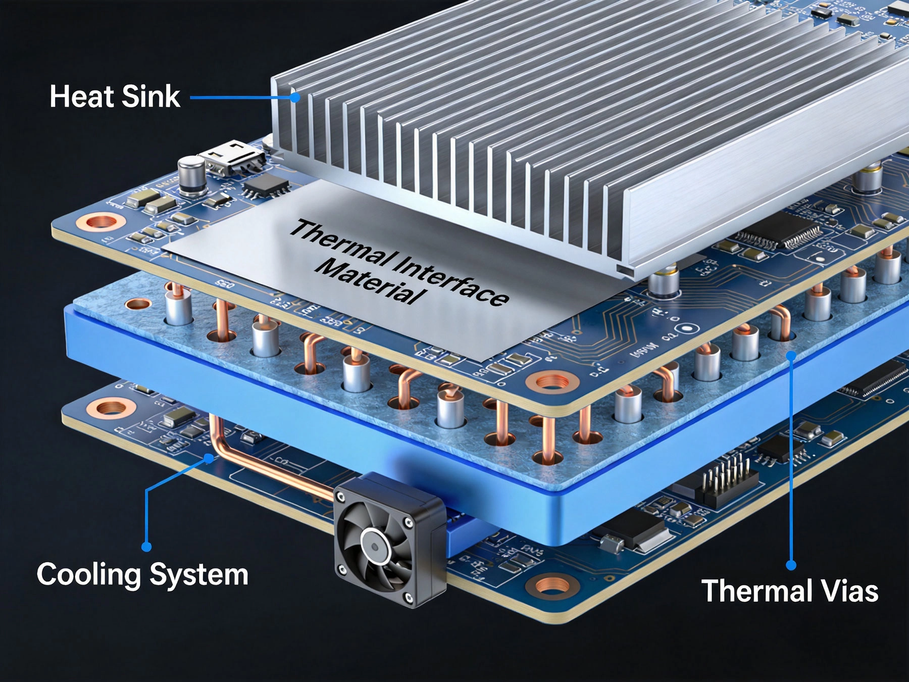
Heat Sink Integration
Heat Sink Attachment Points
Effective heat sink integration requires board-level design:
- Dedicated copper areas: Provide large copper pours under heat sink mounting points
- Thermal via arrays: Dense via arrays under heat sink areas conduct heat to opposite layers
- Mechanical clearance: Ensure component clearance for heat sink dimensions and mounting hardware
- Thermal interface materials (TIM): Provide adequate space for thermal paste or thermal pads between component and heat sink
Heat Sink Selection
Match heat sink to application:
- Pin-fin heat sinks: High surface area, effective for forced convection applications
- Plate-fin heat sinks: Cost-effective, adequate for natural convection
- Heat pipes: For applications requiring heat transport away from sources
- Heat spreaders: Flat metal plates that spread heat across larger areas before convection
Advanced Thermal Management Techniques
Thermal Interface Materials (TIM)
Proper TIM selection bridges thermal gaps:
- Thermal paste: Silicone-based compounds filling microscopic gaps; excellent for high-performance applications
- Thermal pads: Compressible polymer pads with thermal conductivity; easier to apply than paste
- Phase change materials: Solid at room temperature, liquefy during operation to fill gaps
- Indium foil: High-performance, soft metal providing excellent thermal contact
Convection Enhancement
Improve air cooling efficiency:
- Forced convection: Add fans to increase airflow and heat removal rate
- Chassis integration: Use enclosure walls as heat sinks with thermal contact to hot components
- Ventilation: Provide adequate inlet and outlet vents for airflow
- Ducting: Guide airflow specifically past hot components
Liquid Cooling Integration
For high-power applications:
- Cold plates: Metal plates with internal fluid channels for heat removal
- Liquid cooling plates: Directly attached to PCBs for high-power density applications
- Heat exchangers: Radiators or liquid-to-air heat exchangers reject heat to ambient
PCB Material Considerations
High-Thermal-Conductivity Materials
Standard FR-4 has poor thermal conductivity (~0.3 W/mK). Alternatives:
- Metal-backed PCBs: Aluminum or copper core boards provide thermal conductivity 100-200× FR-4
- Ceramic substrates: Excellent thermal conductivity for high-power applications
- Thermally enhanced FR-4: Standard FR-4 with thermal conductivity improvements
Dielectric Thickness Optimization
Thinner dielectrics improve heat transfer:
- Thinner cores: Reduce thermal resistance between copper layers
- Multiple thin cores: More, thinner cores improve layer-to-layer thermal transfer
- Copper-to-copper spacing: Minimize spacing for better thermal conduction
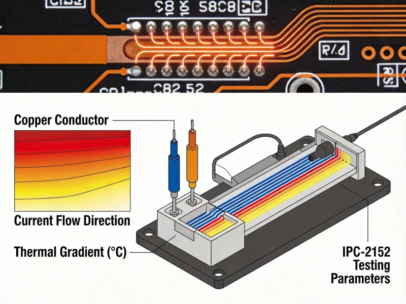
Thermal Analysis and Simulation
Thermal Modeling
Predict temperature rise before fabrication:
- 3D thermal simulation: Model entire PCB with components to predict temperature distribution
- Finite element analysis (FEA): Detailed thermal modeling of complex geometries
- CFD simulation: Computational fluid dynamics for convection optimization
Validation and Testing
Verify thermal performance:
- Thermal imaging: Infrared cameras identify hot spots and verify design assumptions
- Thermocouple placement: Precise temperature measurements at critical locations
- Ambient condition testing: Test across expected ambient temperature range
- Load variation testing: Verify thermal performance across operating range
Common Thermal Management Mistakes
Inadequate Copper Weight
Underestimating Copper Weight needs:
- Using 1oz copper when 2-4oz is needed for power traces
- Neglecting copper pours around power components
- Using thermal reliefs in thermal paths unnecessarily
Insufficient Thermal Vias
Failing to leverage thermal via arrays:
- Not using thermal vias at all under high-power components
- Using too few vias or inadequate via diameter
- Neglecting to connect via arrays to multiple internal layers
Component Placement Issues
Layout decisions compromising thermal performance:
- Concentrating all power components in one area
- Placing temperature-sensitive components near heat sources
- Blocking airflow with component placement or mechanical constraints
Ignoring Thermal Interface
Poor heat sink integration:
- Neglecting to provide adequate copper under heat sinks
- Failing to use appropriate thermal interface materials
- Improper heat sink mounting or contact pressure
Design Checklist
Before finalizing your power Pcb Design, verify:
- Adequate Copper Weight for all power traces (minimum 2oz, preferably 4-6oz for high-current paths)
- Thermal via arrays under all high-power components (minimum 25-50 vias per square inch)
- Internal ground planes for thermal spreading (minimum one full ground plane, preferably multiple)
- Component placement distributes heat sources across the board
- Clear thermal paths from hot components to heat sinks or chassis
- Appropriate thermal interface materials specified for all heat sink attachments
- Airflow considerations integrated into enclosure design
- Thermal Analysis or simulation performed for critical applications
- Thermal test plan defined for prototype verification
Key Takeaways
- Copper weight is the most impactful thermal design factor; use 2-6oz copper for power paths
- Thermal via arrays under high-power components can reduce temperatures 20-40°C
- Internal ground planes provide excellent thermal spreading and should be used whenever possible
- Component placement significantly affects thermal performance; distribute heat sources and consider airflow
- Heat sink integration requires board-level design including copper areas and via arrays
- Thermal interface materials bridge critical thermal gaps and should never be omitted
- Metal-backed PCBs provide dramatic thermal improvements but at higher cost
- Thermal simulation and analysis prevent costly redesigns by identifying issues early
- Validate thermal performance with thermal imaging and thermocouple testing
- Systematic thermal design approach delivers better results than reactive troubleshooting
Frequently Asked Questions
How many thermal vias do I need under a power MOSFET?
The number of thermal vias depends on MOSFET power dissipation and board thermal requirements. As a starting point, use 25-50 vias per square inch under the drain tab. For devices dissipating more than 5W, consider 50-100 vias per square inch. Larger diameter vias (0.5-0.6mm) conduct more heat per via, while smaller vias (0.3mm) allow denser arrays. For critical applications, perform thermal simulation or testing to determine the optimal via density for your specific design.
When should I use metal-backed PCBs instead of standard FR-4?
Metal-backed PCBs (aluminum or copper core) are justified when: thermal conductivity requirements exceed FR-4 capabilities (>1W/m²-K), power density is very high (multiple high-power devices in small areas), or you need direct thermal contact to heat sinks or chassis. If standard FR-4 with heavy copper, thermal vias, and adequate heat sinking achieves your temperature requirements, metal-backed boards represent unnecessary cost. For applications above 10-20W per square inch, metal-backed boards often become cost-effective.
How much does copper weight actually reduce temperature rise?
Copper weight improvements deliver 15-40°C temperature reduction depending on application. Moving from 1oz to 2oz copper might reduce temperature 5-10°C for typical power traces. Moving from 2oz to 4oz might deliver an additional 10-15°C reduction. The exact impact depends on trace geometry, ambient conditions, and overall thermal design. For power semiconductor pads, heavier copper combined with thermal vias can reduce junction-to-ambient thermal resistance by 20-30%, translating to significant temperature reduction.
Should I use thermal paste or thermal pads for heat sink attachment?
Thermal paste provides superior thermal performance (lower thermal resistance) but requires more careful application and can be messy. Thermal pads offer easier application, consistent thickness, and less mess but typically have 2-5× higher thermal resistance than high-quality paste. Use thermal paste for high-performance applications where maximum heat transfer is critical. Use thermal pads for applications where application ease, rework, or mess concerns outweigh thermal performance needs. For most Power Electronics applications below 50W per device, quality thermal pads provide adequate performance.
How do I determine if thermal vias are making a difference?
Compare designs with and without thermal vias, or with varying via densities. Use thermal imaging to measure component and board surface temperatures. Measure junction temperature directly if components have thermal diodes. Compare temperature rise at specific power dissipation levels. In practice, well-designed thermal via arrays under high-power components typically reduce component temperature 15-40°C compared to designs without vias. The benefit is most dramatic for surface-mount components where heat must conduct through the PCB thickness to reach ground planes.
Effective thermal management is essential for reliable Power Electronics Design. By implementing systematic thermal design approaches—heavy copper, thermal vias, internal planes, strategic component placement, and appropriate heat sink integration—you can achieve dramatic temperature reduction without increasing board size significantly. Remember: thermal management should be part of the initial design process, not an afterthought added when prototypes overheat.