

Emi problems in motor driver designs can cause system failures, regulatory rejections, and weeks of expensive debugging.
Motor drivers are among the most Emi-challenging circuits you'll ever design. High currents switching at tens of kilohertz create perfect conditions for electromagnetic interference. The combination of fast switching edges, high di/dt loops, and sensitive control electronics creates a battleground where good designs fail and great designs succeed.
In this guide, we'll explore proven techniques for designing High Current PCB motor drivers that avoid EMI pitfalls, pass regulatory testing, and operate reliably in real-world conditions.
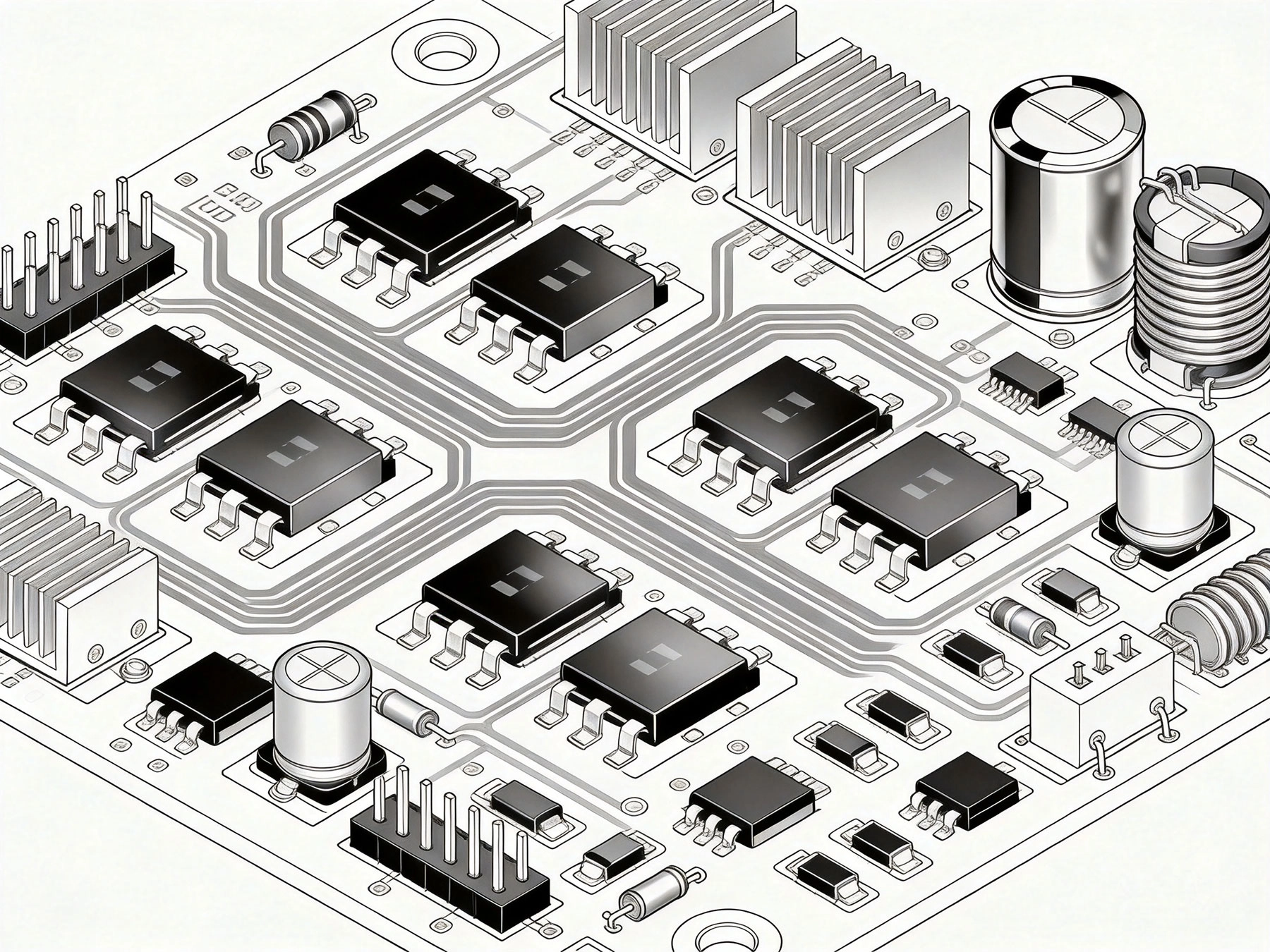
Electromagnetic interference in motor drivers isn't just an inconvenience, it can cause complete system failure. Consider what happens inside a typical motor driver:
These conditions create enormous di/dt (current change over time) and dv/dt (voltage change over time) values. By basic physics, changing currents and voltages create electromagnetic fields. Fast changes create broad frequency spectra that can interfere with anything nearby.
Addressing EMI after discovering problems is expensive. Redesign cycles, shielding additions, and debugging sessions can delay projects by months. The solution is designing for EMI compliance from the start.
Effective EMI control starts with understanding where interference originates:
The primary EMI source in motor drivers is the high-current switching loop. When a MOSFET turns on or off, current must transfer between different paths extremely quickly. This loop includes:
The faster the switching and higher the current, the more EMI this loop generates. Minimizing Loop Area directly reduces emissions.
Motor terminals experience large voltage swings during switching. These swinging nodes act as antennas, radiating high-frequency energy. The motor cable itself can become an efficient radiator at certain frequencies.
Gate driver circuits switch at high frequencies to control power MOSFETs. Fast gate drive signals, while beneficial for efficiency, create their own EMI sources. Gate driver loops can be significant contributors if not carefully routed.
High Current return paths that share traces with sensitive signals create ground bounce. This common-impedance coupling injects noise directly into control circuits.
Pcb Layout is your most powerful EMI control tool. Good layout can eliminate 80% of EMI problems before they occur.
The most critical layout principle: minimize the area enclosed by high current switching loops. Every square millimeter of Loop Area adds to EMI.
Implementation techniques:
Consider this: a 10mm x 20mm loop carrying 20A switching in 50ns generates significant magnetic field energy. Reducing that loop to 5mm x 10mm cuts emissions roughly in half.
One of the most common EMI pitfalls is mixing power ground currents with signal ground returns. High-current motor returns flowing through thin signal ground traces create voltage drops that appear as noise on sensitive circuits.
Best practice:
For multilayer designs, dedicate entire layers to ground. Solid ground planes provide:
Split ground planes are sometimes necessary, but they create EMI risks. If splits are required, ensure no signal traces cross the split, as return currents would be forced to take detoured paths, creating loop antennas.
Thoughtful Component Placement reduces EMI by minimizing path lengths:
A good placement strategy considers current flow. Trace the path from DC input through capacitors, through MOSFETs, to motor outputs. Minimize every segment.
Component choices significantly impact EMI performance:
Bus capacitors smooth DC voltage during switching transients. For EMI, their impedance at switching frequencies matters most.
Selection guidelines:
Typical designs use parallel combinations: 10μF-100μF electrolytic for bulk, plus 0.1μF-1μF ceramic for high frequencies. This combination provides low impedance across the frequency range where EMI matters.
Gate resistors control Mosfet Switching speed. Slower switching reduces EMI but increases power dissipation. The tradeoff requires careful balancing.
Optimization approach:
Typical values range from 1Ω to 22Ω, depending on MOSFET characteristics and EMI requirements.
MOSFET characteristics directly affect EMI:
For EMI-sensitive applications, consider MOSFETs optimized for moderate switching speeds rather than maximum speed.
Grounding in motor driver PCBs requires special attention. Poor grounding is the root cause of many EMI problems.
High frequency currents return directly beneath their signal traces, following the path of least inductance. Low frequency currents follow the path of least resistance. For motor drivers, high frequency switching currents dominate.
This means:
Current sense resistors in motor driver designs present a grounding challenge. The resistor is in the high-current path, but you need to measure voltage across it accurately.
Best practices:
Motor controllers typically include both analog circuits (current sensing, position feedback) and digital circuits (microcontroller, communication). These require different grounding approaches:
When layout and component selection can't fully solve EMI, shielding and filtering become necessary.
Motor cables often act as antennas. Common-mode chokes on motor outputs suppress common-mode currents that would otherwise radiate from cables.
Selection criteria:
Signal lines leaving the motor driver board can carry EMI. Ferrite beads attenuate high-frequency noise:
Metal enclosures provide significant Emi Reduction. When used properly:
RC snubber circuits across MOSFETs dampen ringing caused by Parasitic Inductance and capacitance. While snubbers improve efficiency and reduce EMI, they also add power dissipation.
Design approach:
Verifying EMI performance requires proper testing:
Before formal certification testing, conduct pre-compliance measurements:
Regulatory standards vary by region and application:
Understand which standards apply to your application and design accordingly from the start.
Experienced designers recognize these recurring mistakes:
Problem: Insufficient bypassing allows DC bus voltage to ring during switching, creating broadband EMI.
Solution: Use enough capacitance to maintain stable DC voltage. Add high-frequency ceramic capacitors directly at MOSFET terminals.
Problem: Long gate drive traces have inductance that slows switching and creates ringing, worsening EMI.
Solution: Place gate drivers within millimeters of MOSFET gates. Use wide traces or multiple parallel traces to reduce inductance.
Problem: Motor cables and power cables act as efficient antennas, radiating EMI beyond what board-level design would predict.
Solution: Add common-mode chokes, ferrite sleeves, or shielded cables. Consider the cable as part of the EMI system.
Problem: Using power ground for current sensing creates ground bounce that corrupts measurements and causes instability.
Solution: Implement dedicated sense connections (Kelvin connections) for accurate Current Measurement.
Problem: Aggressive switching speeds that maximize efficiency can create severe EMI problems.
Solution: Balance switching speed against EMI requirements. Use gate resistors or slower gate drivers when EMI is critical.
Designing High Current PCB motor drivers that avoid EMI pitfalls requires understanding the physics, applying proven layout techniques, and making informed component choices. The investment in proper EMI design pays dividends in regulatory compliance, system reliability, and avoided debugging time.
Key principles to remember:
Motor driver EMI challenges are solvable. Successful designs emerge from understanding the sources, applying systematic mitigation techniques, and verifying performance through testing.
Need help with your motor driver Pcb Design? Work with experienced PCB manufacturers and EMI consultants who understand Power Electronics. Their guidance can save months of debugging and ensure your design passes regulatory requirements on the first attempt.
High Current PCB Pad Design: Reinforced Plating vs. Standard PadsJuly/28/2026
Why Your High-Power PCBs Overheat (And the 5 Methods That Actually Fix It)May/20/2026
2oz vs. 4oz Copper: Which is Best for Your High Current PCB?July/10/2026
High Current PCB Design for Medical Imaging EquipmentSeptember/10/2026
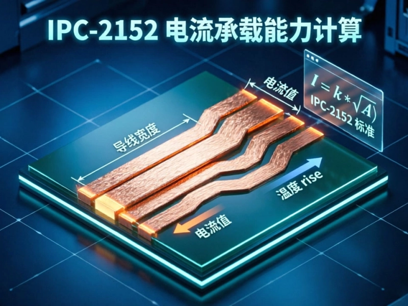
Mastering IPC-2152 Current Carrying Capacity Calculation for Reliable PCB DesignJune/04/2026
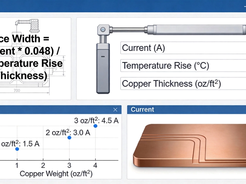
High Current PCB Trace Width Calculator: The Ultimate Engineering GuideMay/20/2026
High Current PCB Design for Railway Traction SystemsAugust/07/2026
High Current PCB Design for Renewable Energy MicrogridsSeptember/30/2026