

Designing a PCB that handles 100 amperes of continuous current is not a straightforward scaling exercise from a 10-ampere board. At 100 amperes, the physics of electrical resistance, Thermal Management, and electromagnetic interference all become simultaneously critical in ways that reshape every aspect of the design. When that board is destined for an Electric Vehicle Battery Management System, the stakes are even higher: the board must operate flawlessly in the demanding thermal and vibration environment of an automotive platform, meet stringent functional safety standards, and remain reliable over a vehicle lifetime measured in hundreds of thousands of miles.
A Battery Management System PCB is at the heart of every Electric Vehicle's electrical architecture. It monitors individual cell voltages and temperatures, balances charge across cell groups, manages charge and discharge currents, and communicates with the vehicle's central control unit to protect the battery pack from overcharge, over-discharge, and thermal runaway. The High Current PCB within the BMS handles the heavy current paths that connect the battery cells to the vehicle's drivetrain inverter and charging infrastructure. Getting this board right is one of the most demanding Pcb Design challenges in the automotive industry.
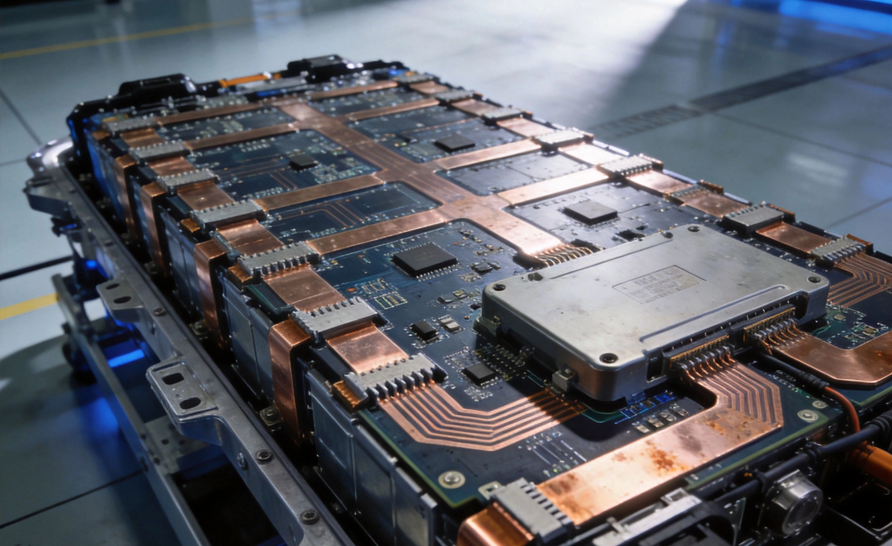
Before diving into the technical details of 100-ampere Pcb Design, it is worth understanding what makes the EV BMS environment uniquely challenging compared to other high-current applications.
Automotive electrical systems operate across a wide voltage range. While the battery pack nominal voltage might be 400 volts for a mid-range EV or 800 volts for a premium model, the Bms Pcb must handle both the high voltage bus and the High Current sense paths simultaneously. The current path may carry 100 amperes or more during fast charging or high-performance acceleration, while simultaneously experiencing voltage transients, load dump events, and electromagnetic interference from the motor inverter switching at frequencies up to 20 kilohertz.
Thermal conditions in an automotive platform are extreme. The battery pack operates in environments ranging from minus 40 degrees Celsius in a Canadian winter to plus 60 degrees Celsius in an Arizona summer. The Bms Pcb must function correctly across this entire temperature range, and it must manage the heat generated by 100 amperes flowing through copper traces even at high ambient temperatures. A board that performs adequately at room temperature may fail catastrophically at 55 degrees Celsius ambient when the additional self-heating pushes component junction temperatures beyond safe limits.
Automotive functional safety requirements add another layer of complexity. BMS systems are typically classified as ASIL-C or ASIL-D under ISO 26262, meaning that a failure in the BMS could result in a safety-critical event. This classification drives requirements for redundant current sensing, dual-verification of critical measurements, and comprehensive diagnostic coverage that goes far beyond what a consumer electronics product would require.
The foundation of any 100-ampere BMS PCB is the stack-up. At this current level, the copper architecture must be designed from the ground up to handle Current Density, thermal spreading, and electromagnetic compatibility simultaneously.
For 100-ampere current paths, standard 1-ounce or even 2-ounce copper is insufficient to keep temperature rises within acceptable limits on practical trace widths. In practice, achieving 100-ampere capability on a PCB typically requires 4-ounce or 6-ounce copper on the current-carrying layers, combined with wide Bus Bar geometries that spread current and heat across a large surface area.
A practical approach is to dedicate entire copper layers in a multilayer stack to Power Distribution. On a 6-layer board, for example, layers 2 and 5 might be solid 4-ounce copper planes dedicated entirely to the positive and negative high-current buses. These plane layers provide massive cross-sectional area for current flow with low resistance and excellent thermal spreading. The signal layers on the top and bottom handle the control circuitry, current sensing, and communication interfaces, while the inner layers provide routing for lower-current signal traces and reference planes.
The challenge with solid plane layers is that they must be segmented to accommodate routing channels for signal traces. Careful planning is needed to ensure that the segmentation does not create narrow bottlenecks in the current path that become hot spots. Using cross-hatching or mesh patterns for the current planes—rather than solid copper fills—can provide a compromise between current capacity and the ability to route signal traces through the plane layer.
The transition between the PCB and the external battery pack connectors is one of the most critical—and most frequently problematic—junctions in a 100-ampere BMS PCB. The connector terminals on the board must handle the full 100-ampere current, and the transition from the wide PCB Bus Bar to the connector pin must not create a resistance hot spot.
Bus Bar Design on the PCB should use wide, flared transitions that gradually narrow from the wide power plane area to the connector landing pad. Sharp corners and abrupt width changes create Current Crowding, which increases local resistance and generates heat at the transition point. A gradual taper from 50 millimeters wide to the connector pin width over a distance of 10 to 20 millimeters distributes the current transition evenly and minimizes hot spots.
Multiple parallel pins for the high-current connectors also help. If the connector uses four pins rated at 30 amperes each, connecting each pin to a dedicated portion of the PCB bus bar ensures that no single junction carries the full 100 amperes. This paralleling approach also provides redundancy—if one pin connection degrades over time, the others can temporarily carry additional current without catastrophic failure.
Managing the heat generated by 100 amperes flowing through a PCB is arguably the most challenging aspect of the design. Every watt of heat that is not removed from the board raises the temperature, and elevated temperatures accelerate all failure mechanisms: solder joint fatigue, connector degradation, dielectric breakdown, and semiconductor failure.
The first line of defense is passive thermal spreading through the PCB structure itself. Copper is an excellent thermal conductor—approximately 400 W/m·K for solid copper—which means that the wide copper bus bars and plane layers that carry current also act as effective heat spreaders. By designing the current-carrying copper to cover as much of the board area as possible, heat generated anywhere on the board can spread laterally across the copper and dissipate from the entire board surface rather than concentrating at the hottest point.
Thermal Vias placed in a grid pattern beneath high-power components—MOSFETs, current sense resistors, and connector termination areas—conduct heat from the component side of the board to any internal copper planes and to the opposite side of the board. A typical thermal via array beneath a high-power component might include 16 to 36 vias per square centimeter, with via diameters of 0.3 to 0.5 millimeters and copper barrel thickness of at least 25 micrometers to maximize thermal conductivity.
For a 100-ampere BMS PCB, passive thermal spreading through the board alone is often insufficient, and direct board-level heat sinking becomes necessary. Aluminum metal-core PCBs (MCPCBs), where the base substrate is an aluminum plate rather than FR-4, provide dramatically better thermal conductivity from the board to the environment. An aluminum core PCB has a thermal conductivity of approximately 1 to 2 W/m·K compared to 0.29 W/m·K for standard FR-4—a factor of 5 to 7 improvement in heat spreading.
The thermal interface between the PCB and the metal enclosure or heatsink must be carefully managed. Using thermal interface material (TIM) with high thermal conductivity, ensuring flat and clean mating surfaces, and applying appropriate mounting pressure through threaded standoffs or PEM fasteners all contribute to effective heat transfer from the board to the heatsink. Gaps or voids in the thermal interface material create Thermal Resistance that can be 10 to 100 times higher than properly applied TIM, so assembly quality control is essential.
In higher-power BMS designs or in vehicle architectures where the battery pack is liquid-cooled, integrating active cooling directly into the Bms Pcb Design can be necessary. This might include designing the board with integral cooling channels, specifying a board that mounts directly to a liquid-cooled cold plate, or specifying fans or blowers for air-cooled designs. Active cooling extends the safe operating current range significantly and may be required for 100-ampere continuous operation in elevated ambient temperature conditions.
The components selected for a 100-ampere BMS PCB must be rated well beyond the nominal operating current to provide safety margins and account for elevated temperatures, transient overloads, and long-term degradation.
Accurate Current Measurement is one of the most critical functions of the BMS PCB. Current sense resistors and hall-effect current sensors are the two primary sensing technologies used in EV BMS applications.
Shunt resistors—precision low-value resistors placed in series with the high-current path—provide the most accurate Current Measurement across a wide temperature range and at reasonable cost. For a 100-ampere BMS, shunt resistors with power ratings of 5 to 10 watts and values in the range of 0.1 to 0.5 milliohms are typical. The power dissipated in the shunt (P = I² × R) at 100 amperes through a 0.5-milliohm shunt is 5 watts—significant self-heating that must be accounted for when specifying the resistor. A shunt that self-heats to 100 degrees Celsius will have a different resistance value than at room temperature, which affects measurement accuracy. Selecting shunts with low temperature coefficients of resistance (TCR) and adequate power derating for temperature is essential.
Hall-effect sensors offer the advantage of no insertion resistance—current flows through a bus bar that passes through the sensor, rather than through a Shunt Resistor. This eliminates the self-heating issue and the associated measurement drift. However, hall-effect sensors have higher offset drift over temperature and may require more careful compensation in the measurement algorithm. For ASIL-D BMS systems, redundant current sensing using both shunt and hall-effect technologies in parallel provides the highest diagnostic coverage.
For BMS designs that include active cell balancing or charge-discharge control, MOSFETs or IGBTs handle the high-current switching. These devices must have on-resistance (Rds-on) low enough to keep self-heating within acceptable limits at the full 100-ampere current level. A MOSFET with 1 milliohm Rds-on dissipates 10 watts at 100 amperes (P = I² × R), which requires a substantial heatsink or active cooling to keep the junction temperature below the maximum rating.
Automotive-grade MOSFETs rated for AEC-Q101 with operating temperatures up to 175 degrees Celsius junction temperature are preferred for EV BMS applications. Silicon carbide (SiC) MOSFETs are increasingly used in high-performance EV BMS designs because of their lower on-resistance, higher thermal conductivity, and superior performance at elevated temperatures compared to silicon MOSFETs. SiC MOSFETs carry a significant cost premium but can substantially reduce heatsink requirements and improve power efficiency.
Connectors for the high-current paths must be rated well above 100 amperes—typically at least 150 to 200 amperes rated current—to provide safety margin and account for connector degradation over the vehicle lifetime. Automotive-grade connectors from manufacturers like TE Connectivity, Amphenol, or Molex that are specifically rated for EV battery pack applications include features like silver-plated contacts for low resistance, high-temperature rated housings, and positive latching mechanisms that prevent vibration-induced disconnects.
The PCB termination of high-current connectors requires careful attention to the joint quality. Soldering a large-gauge connector pin to a Heavy Copper pad on the PCB creates a thermal challenge—the dissimilar thermal expansion rates of the connector metal and the PCB substrate can stress the solder joint during Thermal Cycling. Using through-hole solder termination rather than surface mount, applying solder preforms for consistent joint volume, and specifying high-temperature solders like SAC305 or high-lead solders for the connector joints all contribute to long-term joint reliability.
Carrying 100 amperes of current generates significant electromagnetic fields, and the switching transients from the motor inverter and Dc-dc Converter in an EV create conducted and radiated interference that the BMS PCB must withstand without performance degradation. EMC design is not optional in automotive applications—meeting CISPR 25 and ISO 11452 conducted and radiated emission limits is a legal requirement for vehicle type approval.
The high-current power loop on the BMS PCB should be designed as a compact, symmetrical geometry that minimizes loop area. A large loop area acts as an antenna, radiating electromagnetic energy that can interfere with the BMS analog measurement circuitry and violate emission limits. Routing the high-current bus as a pair of parallel wide traces on adjacent layers—with positive on one layer and negative directly beneath on the next—creates a tightly coupled transmission line with minimal loop area and excellent self-shielding.
Separation between high-current power traces and sensitive analog measurement circuits is equally important. The magnetic field generated by 100 amperes can induce noise voltages in nearby signal traces, degrading the accuracy of cell voltage measurements or current sense readings. Using dedicated ground reference layers between power and signal areas, routing signal traces perpendicular to power traces rather than parallel, and maintaining physical separation of at least 5 millimeters between high-current paths and sensitive analog nodes all help minimize EMI coupling.
High-frequency switching noise from the vehicle's Power Electronics propagates into the BMS through the power supply rails. Decoupling capacitors placed immediately adjacent to the power pins of every IC—typically 100 nanofarad ceramic capacitors in parallel with 10-microfarad tantalum or film capacitors for bulk decoupling—filter this noise and prevent it from corrupting analog measurements. For the current sense amplifiers, differential filtering using matched RC networks on both the positive and negative sense inputs attenuates common-mode noise while preserving the differential current signal.
An EV BMS PCB must meet a demanding set of automotive quality and safety standards that go far beyond the requirements for consumer or industrial electronics.
AEC-Q100 and AEC-Q101 define the qualification requirements for integrated circuits and discrete semiconductors used in automotive applications. Components specified for the BMS must meet these qualification standards, which include accelerated life testing, temperature cycling, mechanical vibration, electrical overstress, and electrostatic discharge testing. Non-qualified components—even if they meet electrical specifications—should not be used in automotive BMS applications.
The PCB itself must be manufactured to IPC Class 3 standards, the highest level of PCB workmanship quality, which specifies stringent requirements for plating thickness, dielectric integrity, solder joint quality, and documentation. For BMS systems in vehicles operating in harsh thermal environments, some manufacturers impose additional internal requirements beyond IPC Class 3 that specify tighter tolerances on critical parameters.
ISO 26262, the functional safety standard for automotive systems, imposes systematic and hardware architecture requirements on the BMS design. For ASIL-C or ASIL-D systems, this typically includes hardware architecture metrics that require either hardware redundancy for critical functions or detailed diagnostic coverage analysis proving that single-point faults are adequately detected and managed. The Bms Pcb Design must support these requirements through features like redundant current sense amplifiers, dual-verified power supply rails, and comprehensive self-test diagnostics that run at startup and periodically during operation.
Traceability from the component level through the Pcb Assembly to the finished vehicle is another ISO 26262 requirement. Every component on the BMS PCB must be traceable to its lot date code and manufacturing source, and this traceability must extend into the vehicle's service records. This traceability requirement affects the PCB design through documentation requirements on the assembly drawing and drives specific component packaging and labeling requirements.
For practical Pcb Trace geometries on an FR-4 board, achieving 100-ampere continuous current capacity with a temperature rise below 30 degrees Celsius above ambient typically requires 4 to 6 ounces of Copper Weight and trace widths of 50 to 100 millimeters. In practice, no single wide trace is used—instead, the current is distributed across multiple parallel layers using solid copper plane areas, Thermal Vias, and parallel connector pins. A single narrow trace on a standard 1-ounce board would require unrealistic widths and would fail thermally.
Yes, significantly. Aluminum metal-core PCBs have thermal conductivity approximately 5 to 7 times higher than standard FR-4, which allows heat to spread laterally from hot spots much more effectively. For a 100-ampere BMS application, a metal-core PCB design can reduce the required Copper Weight and trace widths while achieving the same or better thermal performance. Metal-core PCBs carry a cost premium and have different assembly process requirements, but for thermally demanding high-current applications, the performance benefit is often worth it.
Preventing connector overheating requires attention to three factors: Current Density in the connector termination, quality of the solder or mechanical joint between the connector and the PCB, and Thermal Management of the connector body itself. Specifying connectors rated at least 50 percent above the nominal operating current, using multiple parallel pins to reduce current per pin, applying solder joints with adequate volume and proper process control, and ensuring adequate airflow or heatsinking over the connector all contribute to reliable operation. Temperature monitoring using embedded thermocouples or infrared sensors in the BMS design allows the system to derate current if connector temperatures approach safe limits.
For ASIL-C systems, hardware architecture metrics require Single-Point Fault metric above 90 percent and Latent Fault metric above 60 percent. For current sensing, this translates to requirements for redundant sensing paths (typically two independent shunt resistors and two independent ADCs), open-circuit and short-circuit detection on every sense path, periodic self-test that injects known currents and verifies measurement accuracy, and plausibility checking between the two redundant channels. The specific implementation must be validated through detailed FMEDA analysis and confirmed through hardware-in-the-loop testing.
Temperature affects BMS measurement accuracy in multiple ways. Shunt resistors have temperature coefficients of resistance that change their value as temperature rises—typically 50 to 100 parts per million per degree Celsius for precision shunts. The analog-to-digital converter (ADC) in the current sense amplifier has input offset drift over temperature that adds to measurement error. The thermoelectric EMK effect at the junction between dissimilar metals in the measurement circuit creates temperature-dependent offset voltages. Each of these error sources must be quantified, and the BMS algorithm must include temperature compensation that corrects for these drifts. For ASIL-C/D systems, the temperature compensation algorithm itself is a safety-critical software element that must be developed to the appropriate safety integrity level.
Designing a 100-ampere PCB for an EV battery management system is one of the most demanding PCB engineering challenges in the industry. It requires simultaneous mastery of high-current thermal management, automotive functional safety standards, electromagnetic compatibility, component qualification, and manufacturing process control. The board must operate reliably at temperatures from minus 40 to plus 85 degrees Celsius, survive the vibration environment of an automotive platform, meet stringent EMI limits, and support safety-critical measurement and control functions for the entire vehicle lifetime.
The key to success lies in taking a system-level approach to the design. The copper architecture, thermal management strategy, component selection, EMC design, and safety architecture must all be designed together, because changes in any one area cascade into the others. A stack-up optimized for thermal spreading may conflict with EMC routing requirements. Component selection that provides excellent electrical performance may fail in thermal testing. The discipline of a 100-ampere BMS design is the discipline of managing these interdependencies and finding solutions that satisfy all requirements simultaneously.
For engineering teams undertaking this challenge for the first time, the investment in early thermal simulation, detailed DFM reviews with the manufacturing partner, and comprehensive component qualification testing before finalizing the design pays dividends in reduced spin count and faster time to production. A board that goes through three design iterations due to thermal surprises or EMC failures costs far more than the engineering time invested in getting it right the first time.
This article is provided for general informational purposes regarding 100-ampere High Current PCB design for EV battery management systems. Automotive safety-critical applications require formal engineering validation, ISO 26262 compliance processes, and manufacturer-specific qualification that go well beyond general design guidelines. Always consult with qualified Automotive Electronics engineers and your vehicle OEM for application-specific requirements.
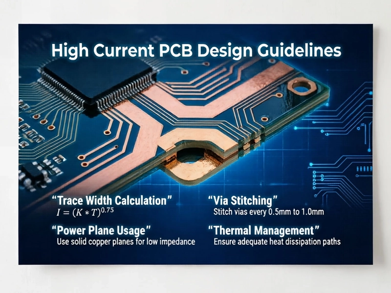
High Current PCB Design Guidelines: Ensuring Reliability and SafetyJune/08/2026
A Deep Dive into High Current PCB Design for Solar InvertersJuly/17/2026
High Current PCB Design for Audio Amplifiers: Avoiding Ground LoopsSeptember/14/2026
High Current PCB Design for Electric Vehicle Charging StationsAugust/15/2026
High Current PCB Design for Aerospace Power DistributionSeptember/08/2026
Designing a High Current PCB for Industrial Welding EquipmentJuly/23/2026

High Current PCB Design for Railway Traction SystemsAugust/07/2026
High Current PCB Design for Uninterruptible Power Supplies (UPS)September/02/2026