

Modern electronic systems demand increasingly higher currents from their Power Distribution networks. From AI servers consuming thousands of watts to Electric Vehicle motor controllers handling hundreds of amperes, the humble printed circuit board has become a critical infrastructure for power delivery. Yet despite advances in semiconductor technology, one persistent challenge continues to haunt PCB designers: voltage drop in Power Planes.
Voltage drop—sometimes called IR drop after the Ohm's law equation V = IR—occurs when the resistance of copper traces and planes causes a measurable reduction in voltage reaching the load. For systems running at 12V or lower, even small voltage drops can push critical components outside their operating specifications, causing system failures, unexpected shutdowns, or degraded performance.
This article presents a comprehensive case study of voltage drop problems encountered in a real high-current Pcb Design, along with the systematic approach used to diagnose and overcome these challenges.
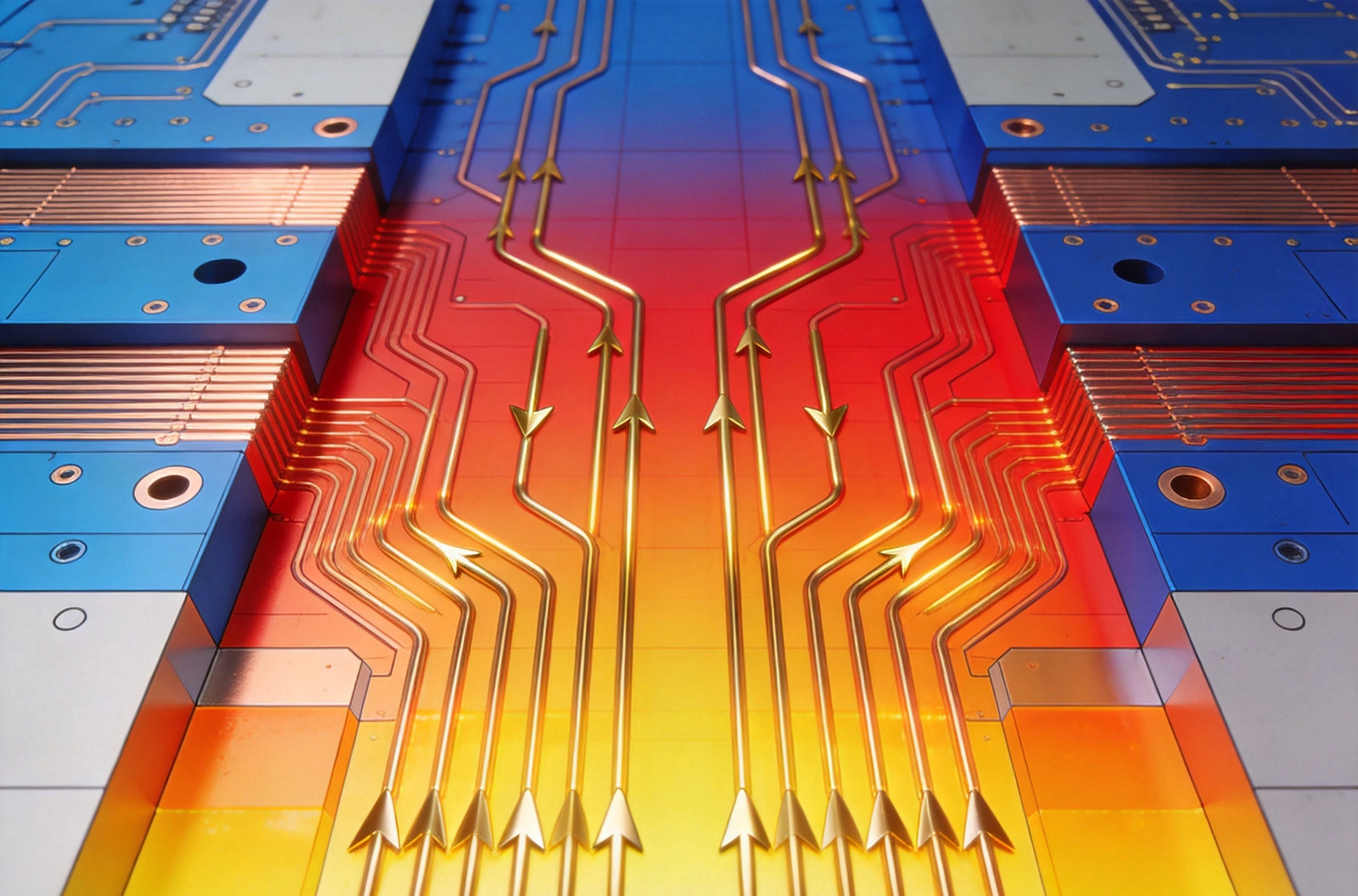
Our case study focuses on a Power Distribution board designed for an industrial automation system. The board receives 48V input from a main power supply and distributes regulated 12V power to multiple load points across the system. The specification requires maintaining 12V ±5% (11.4V to 12.6V) at all load locations while delivering up to 30 amperes of continuous current.
Initial design assumptions predicted minimal voltage drop due to the relatively short trace lengths involved. However, prototype testing revealed significant problems:
With a 1.3V drop across the board at maximum current, this design would fail compliance testing and likely cause downstream system failures.
Before implementing solutions, we needed to understand why the voltage drop was occurring. The resistance of a Copper Trace or plane depends on three factors:
The formula R = ρ × L / A reveals why Power Planes fail: as current travels across a plane toward a distant load, the effective cross-sectional area available for current flow decreases, causing resistance to increase along the path.
Our thermal imaging analysis revealed another problem: uneven Current Distribution across the power plane. Current tends to crowd into narrow paths, particularly around vias and connection points. This Current Crowding increases local resistance and generates hotspots that threaten reliability.
The power plane, while appearing continuous, was effectively acting like multiple narrow conductors in parallel rather than a uniform low-resistance path. This is a common misconception in Pcb Design—designers often assume a solid plane provides uniform Current Distribution, when in reality current takes the path of least resistance, which often means crowded paths through vias and narrower sections.
Each via connecting the power plane to component pads adds resistance to the current path. Standard 0.4mm diameter through-hole vias typically contribute 0.5mΩ to 1mΩ of resistance depending on plating thickness. For a design with multiple vias carrying significant current, these individual resistances add up to measurable voltage drop.
In our case, the 8 vias connecting the input connector to the main power plane were carrying the full 30A current, creating a significant resistance bottleneck at a single point.
The first and most straightforward solution involved increasing Copper Weight from the standard 1oz (35μm) to 2oz (70μm). Doubling Copper Thickness directly halves the resistance of any given trace or plane section.
For our power distribution application, the impact was significant. Initial calculations showed:
Beyond the electrical benefits, heavier copper provides better thermal conductivity, helping to dissipate heat generated by current flow. This improves both electrical performance and long-term reliability.
The original design used wide traces to distribute power, treating the plane as incidental routing. The redesigned board implements dedicated power planes on two internal layers, connected with multiple Thermal Vias to create a low-resistance network.
Key changes included:
The parallel path strategy proved particularly effective. By creating multiple redundant current routes from input to output, no single path carries the full current burden. This reduces resistance, distributes heat generation, and provides fault tolerance if a connection point fails.
Instead of relying on a few large vias, we implemented via-in-pad technology with arrays of smaller vias at high-current connection points. This approach provides several advantages:
For the main input connection, we implemented an array of 12 vias (0.5mm diameter) where a single 1.2mm via was originally specified. Current testing showed via resistance dropped from 0.8mΩ to 0.15mΩ—a 5× improvement.
For the most critical load points, we implemented remote sense lines that allow voltage regulation circuits to measure voltage directly at the load rather than at the source. This technique, common in power supply design, compensates for voltage drop in the distribution path by increasing source voltage to ensure adequate voltage at the load.
While effective, remote sensing requires careful implementation:
High-current power planes generate significant heat. Ohm's law (P = I²R) tells us that reducing resistance also reduces power dissipation and heat generation. However, even optimized designs require Thermal Management considerations.
Our revised design incorporates several thermal improvements:
Thermal simulation using finite element analysis (FEA) tools predicted maximum temperatures under worst-case conditions. The optimized design maintained temperatures below 85°C at 25°C ambient, compared to 120°C+ with the original design.
After implementing these changes, the revised board underwent rigorous testing:
The maximum voltage drop dropped from 1.3V to 0.25V, a reduction of over 80%. At 30A maximum current, this translates to total dissipation in distribution resistance of just 7.5W compared to 39W previously.
Thermal imaging confirmed the improvements:
Based on this case study, several principles emerge for designing high-current power distribution systems:
Designers should model actual current flow paths, not just electrical connections. Current follows physics, not design intent, and will take unexpected routes through available copper if main paths are restricted.
Whenever possible, dedicate entire PCB layers to power distribution. Planes provide lower resistance, better thermal performance, and more uniform current distribution than even very wide traces.
Don't rely on single-point connections. Multiple parallel paths through different PCB layers, connected with abundant stitching vias, provide redundancy and reduce overall impedance.
Copper resistance increases approximately 0.4% per °C above 20°C. A design that meets specifications at room temperature may fail at elevated operating temperatures. Always analyze at worst-case temperature conditions.
Power requirements tend to increase during product development. Designing for 50% more current capacity than initially required provides headroom for changes without PCB redesign.
Voltage drop in High-current Pcb power planes is a solvable problem, but it requires understanding both the electrical physics and practical design techniques. This case study demonstrates that systematic diagnosis—combining calculation, simulation, and testing—leads to effective solutions.
The key is treating power distribution as a first-class design challenge rather than an afterthought. By implementing dedicated power planes, optimizing via configurations, and designing for current flow rather than mere connectivity, engineers can achieve reliable high-current performance in even demanding applications.
As power requirements continue to increase across industries—from AI computing to electric vehicles—the importance of proper power plane design will only grow. Engineers who master these techniques will be well-positioned to tackle next-generation power distribution challenges.
Acceptable voltage drop depends on system requirements. General guidelines suggest limiting total distribution drop to 3-5% of nominal voltage for most applications. For critical systems with tight regulation requirements, drops below 1% may be necessary. Always verify against component datasheet specifications for minimum operating voltage.
Use the resistance formula R = ρ × L / A for each conductor segment, where ρ is copper resistivity (1.68 × 10⁻⁸ Ω·m), L is length in meters, and A is cross-sectional area in square meters. Sum resistance values along the current path, then multiply total resistance by load current to get voltage drop. For vias, use manufacturer data or measure resistance directly.
For high-current applications above 10A, 2oz copper (70μm) is typically the minimum recommended weight. Applications above 30A may benefit from 3oz or even 6oz copper, though this requires specialized manufacturing. Consider using bus bars or wire attachments for currents exceeding 50A rather than PCB copper alone.
Thermal vias improve Current Carrying Capacity by providing additional paths from component pads to internal planes and by improving thermal conductivity. However, thermal vias also reduce available copper area around pads. Use multiple small vias in arrays rather than fewer large vias to maximize current capacity while maintaining thermal benefits.
Power planes are dedicated, solid copper layers assigned to specific voltages, typically on internal PCB layers. Copper pours are filled areas on outer layers that may connect to planes or serve as supplementary ground/thermal connections. While pours help, they cannot match the performance of dedicated internal planes for high-current distribution.
High Current PCB Solder Wicking: Tented Vias vs. Untented ViasSeptember/01/2026
High Current PCB Routing: 45-Degree Angles vs. Curved Traces in PracticeJuly/12/2026
High Current PCB Grounding: Star Ground vs. Ground Plane in High Current PathsJuly/31/2026
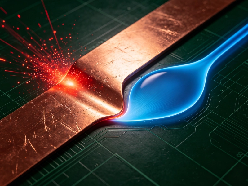
High Current PCB Current Crowding: Sharp Corners vs. Teardrop TransitionsSeptember/03/2026
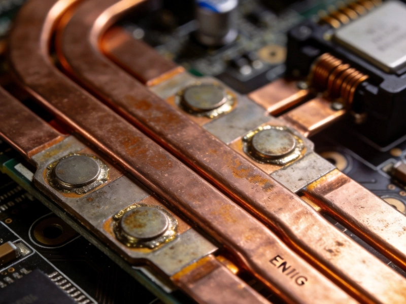
High Current PCB Surface Finish: ENIG vs. HASL for High Current PadsSeptember/23/2026
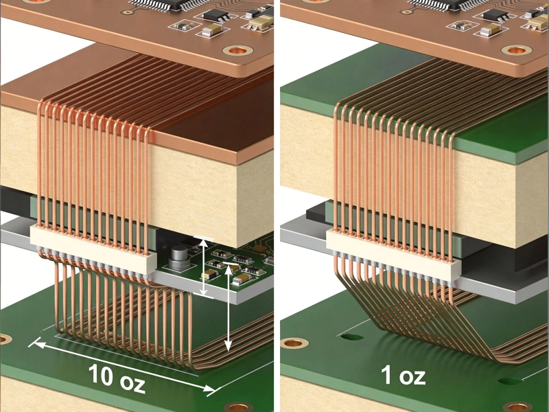
Heavy Copper vs Standard Copper PCB: Complete Comparison Guide for EngineersMay/20/2026
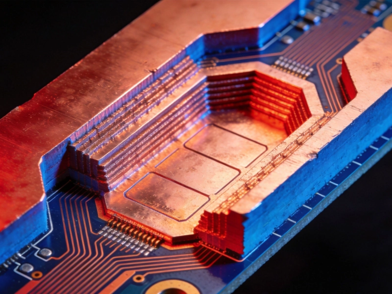
High Current PCB Embedded Copper: Internal vs. External Heat DissipationSeptember/26/2026

Building a High Current PCB Power Supply for Server RacksJuly/30/2026