
Plated through holes (PTH) are critical components of modern printed circuit boards, enabling electrical connections between different layers, providing mechanical support for through-hole components, and facilitating signal and power transmission across the PCB stackup. One of the most important design considerations when working with PTHs is their current rating (or ampacity) – the maximum amount of current a plated through hole can safely carry without exceeding temperature limits or causing premature failure.
Understanding PTH current rating is essential for designing reliable PCBs, especially for high-power applications like power supplies, motor controllers, automotive electronics, and industrial equipment. In this comprehensive guide, we'll break down the key factors that affect plated through hole Current Carrying Capacity, explain how to calculate and optimize PTH ampacity, and share proven design best practices to ensure your PCB designs operate reliably over their entire lifecycle.
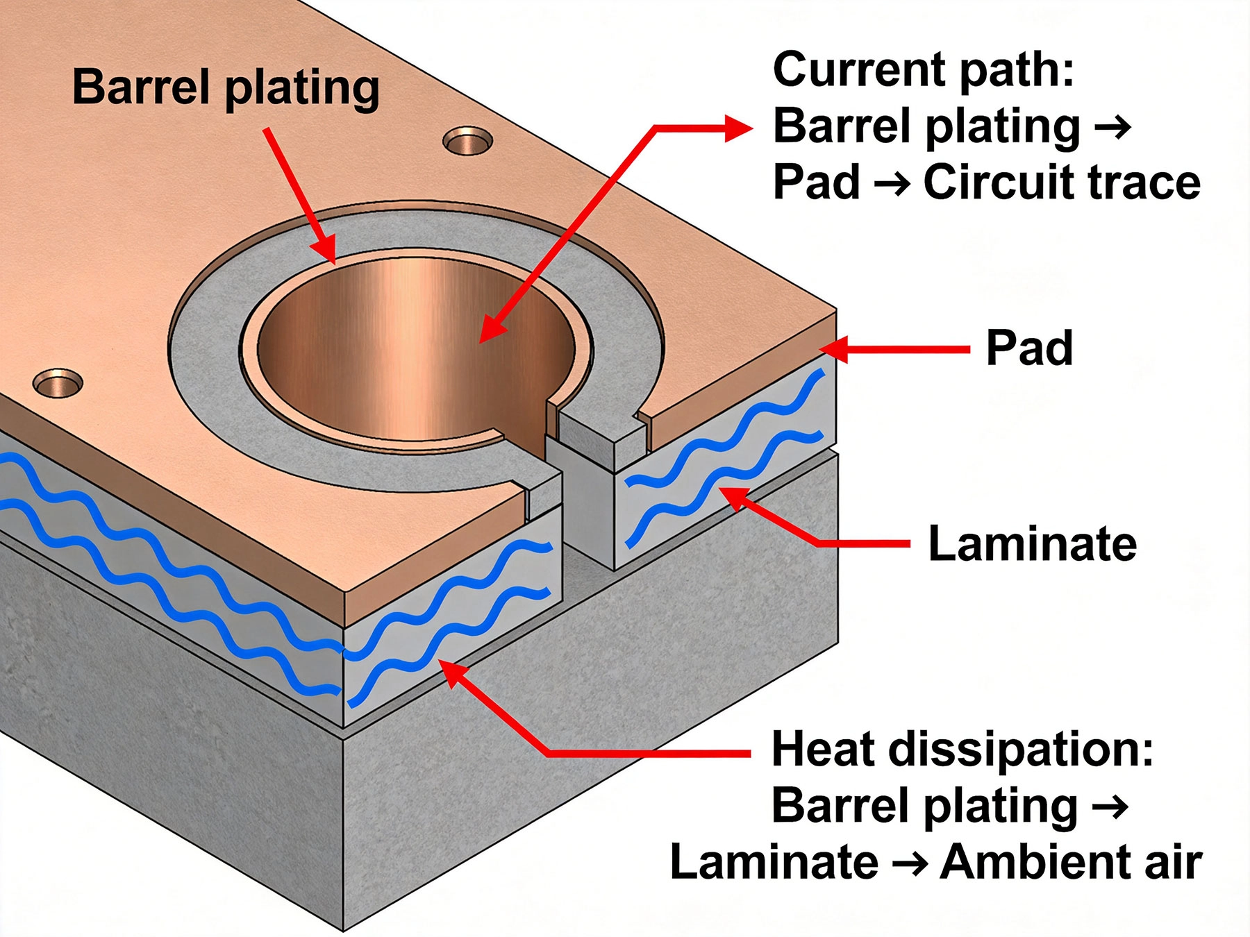
Plated through holes are copper-plated holes drilled through the entire thickness of a PCB. During manufacturing, after drilling, a thin layer of copper is deposited onto the inner walls of the hole, creating a conductive path that connects copper traces on different layers of the board. PTHs serve three primary purposes:
Unlike non-plated through holes (NPTH), which are used for mechanical mounting only, PTHs are electrically conductive, making their Current Carrying Capacity a critical design parameter for all types of PCB applications.
The maximum current a plated through hole can safely carry depends on multiple interconnected factors. Ignoring any of these factors in your design can lead to overheating, thermal stress, premature PTH failure, or even catastrophic PCB damage.
The most significant factor affecting PTH current rating is the cross-sectional area of the copper plating on the hole walls. Larger diameter holes have more surface area for current flow and Heat Dissipation, allowing them to carry higher currents. A 0.8mm diameter PTH can typically carry 2-3 times more current than a 0.4mm diameter PTH with the same plating thickness.
The thickness of the copper plating on the PTH walls directly impacts its current carrying capacity. Standard plating thickness ranges from 20μm (0.8 mils) to 35μm (1.4 mils) for most commercial applications, while high-current designs may require 50μm (2 mils) or thicker plating. Thicker plating provides a larger conductive cross-section, reducing resistance and improving Heat Dissipation.
Current ratings are always specified at a particular ambient temperature. As operating temperature increases, the maximum allowable current decreases, because copper's electrical resistance increases with temperature, leading to more I²R heating. Most PTH current ratings are specified for a maximum temperature rise of 10°C, 20°C, or 30°C above ambient temperature.
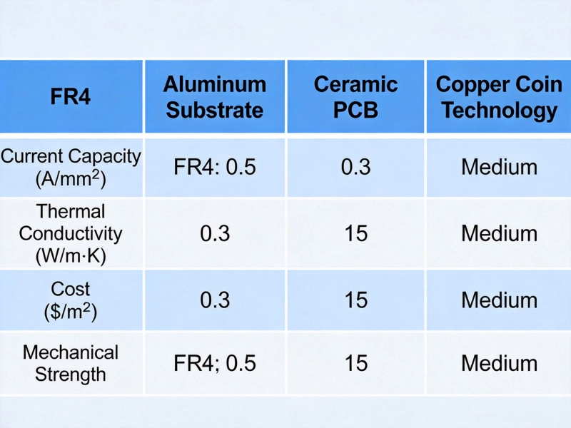
The PCB substrate material affects how efficiently heat can dissipate away from the PTH. High-thermal-conductivity materials like aluminum-backed PCBs or ceramic substrates can significantly improve PTH current carrying capacity compared to standard FR-4, as they conduct heat away from the hole more effectively.
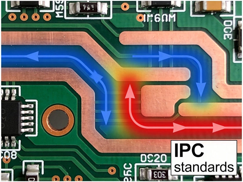
The width and Copper Weight of the traces connected to the PTH also impact its effective current rating. If the connecting traces are too narrow, they will act as a bottleneck, limiting the total current that can safely flow through the circuit even if the PTH itself has a higher ampacity.
PTHs that connect to more copper layers generally have higher current ratings, as the additional copper provides more surface area for heat dissipation and parallel current paths. A PTH connected to four internal copper planes can carry significantly more current than an identical PTH connected only to the top and bottom layers.
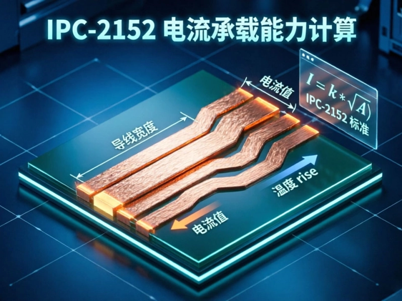
The Ipc-2152 standard (Standard for Determining Current Carrying Capacity in Printed Board Designs) provides the most widely accepted methodology for calculating PTH current ratings. Unlike older IPC standards that used simplified formulas, Ipc-2152 takes into account multiple factors including plating thickness, hole diameter, temperature rise, and PCB material properties.
For quick estimations, you can use the following simplified formula to get a rough idea of PTH current carrying capacity:
I = 0.048 * A^0.44 * ΔT^0.725
Where:
I = Maximum current in Amps
A = Cross-sectional area of the PTH copper plating in mils²
ΔT = Maximum allowable temperature rise in °C above ambient
To calculate the cross-sectional area (A) of the PTH plating:
A = π * (D - t) * t
Where:
D = Hole diameter in mils
t = Copper plating thickness in mils
For a 0.8mm (31.5 mil) diameter PTH with 25μm (1 mil) plating thickness, allowing a 20°C temperature rise:
Note that this is a simplified estimate – for production designs, you should always use IPC-2152 compliant calculation tools or consult with your PCB manufacturer for accurate current rating values based on their specific manufacturing processes.
Many free and commercial online calculators are available that implement the full IPC-2152 methodology, including:
Even experienced PCB designers often make mistakes when calculating and specifying PTH current ratings, leading to reliability issues in production. Here are the most common pitfalls to avoid:
Many designers use the exact calculated maximum current rating for their PTHs, leaving no safety margin for manufacturing variations, unexpected operating conditions, or component degradation over time. Best practice is to use a minimum 25% design margin, and 50% or more for high-reliability applications.
PCB manufacturers typically specify plating thickness as a minimum value, with actual plating thickness varying across the board and between production runs. Always use the minimum specified plating thickness for your calculations, not the nominal or maximum possible value.
When multiple high-current PTHs are placed close together, their heat output can add up, leading to higher local temperatures than individual PTHs would produce in isolation. Space high-current PTHs at least 2-3 times their diameter apart to minimize thermal coupling effects.
Via-in-pad designs, where PTHs are placed directly under component pads, can have reduced current ratings due to limited heat dissipation, especially if the vias are filled with non-conductive material. Consult with your manufacturer for specific current rating adjustments for via-in-pad designs.
Always use the actual maximum ambient temperature your product will operate in when calculating current ratings, not the standard 25°C laboratory ambient. For automotive under-hood applications, for example, ambient temperatures can reach 125°C or higher, significantly reducing allowable current.
Follow these proven design best practices to ensure your PTH designs operate reliably even under high-current conditions:
For power paths carrying more than 5A, use larger diameter PTHs than you would for signal paths. A 1.0mm or 1.2mm diameter PTH will provide significantly higher current capacity and improved reliability compared to a standard 0.6mm or 0.8mm PTH.
For high-current applications, specify a minimum 30μm (1.2 mil) copper plating thickness for PTHs, and consider 50μm (2 mil) plating for currents above 10A. Work with your PCB manufacturer to ensure they can consistently achieve the required plating thickness across all holes.
For currents above 15A, consider using multiple identical PTHs in parallel to share the current load. This not only increases total current carrying capacity but also provides redundancy in case of individual PTH failure. Ensure each PTH is connected to adequate copper area on all layers to balance current sharing.
Connect high-current PTHs to large copper pours or planes on as many layers as possible to improve heat dissipation. Thermal Vias placed close to high-current PTHs can also help conduct excess heat away to inner layers or heat sinks.
Always use IPC-2152 compliant calculation methods rather than outdated rules of thumb. The IPC-2152 standard has been extensively tested and validated against real-world PCB performance, providing much more accurate current rating values than older simplified formulas.
For high-power or high-reliability designs, perform thermal simulation during the design phase to identify potential hot spots around high-current PTHs. Once prototypes are available, perform actual current testing under worst-case operating conditions to validate your design.
A: A standard 0.8mm diameter PTH with 25μm plating on FR-4 can typically carry 5-8A with a 20°C temperature rise, depending on connected copper area and operating conditions.
A: No, vias (which are typically smaller and may be tented or filled) usually have lower current ratings than equivalent size PTHs. Always calculate via current ratings separately using appropriate formulas.
A: As ambient temperature increases, the maximum allowable current decreases. For example, a PTH rated for 10A at 25°C ambient may only be able to carry 7A at 85°C ambient with the same temperature rise limit.
A: Yes, for aerospace, automotive, or medical applications, derate PTH current ratings by 30-50% to provide additional safety margin and ensure long-term reliability.
A: No, tinning (applying solder to PTH walls) does not significantly increase current rating, as solder has much higher electrical resistance than copper. The primary current carrying path is always the copper plating.
Properly specifying plated through hole current ratings is a critical aspect of reliable Pcb Design, especially for high-power applications. By understanding the factors that affect PTH ampacity, using IPC-2152 compliant calculation methods, and following proven design best practices, you can ensure your PCB designs will operate safely and reliably over their intended lifecycle.
When in doubt, always consult with your PCB manufacturer early in the design process to verify current rating assumptions and confirm that your specified PTH dimensions and plating requirements can be consistently achieved within your production budget. Taking the time to properly optimize your PTH design during the early design stages will help avoid costly redesigns, production delays, and field failures later.
Need help with your high-current PCB design? Our team of experienced PCB design engineers can help you optimize your PTH and via designs for maximum reliability and performance. Contact us today for a free design review and consultation.
Plated Through Hole Current Rating: Complete Guide for PCB DesignersMay/21/2026
High Current PCB Design GuidelinesMay/21/2026
Why Your High-Power PCBs Overheat (And the 5 Methods That Actually Fix It)May/20/2026
Best Material for High Current PCB DesignMay/21/2026
Bus Bar vs PCB Trace for High CurrentMay/21/2026
How Much Current Can a PCB Trace Carry? Complete Engineering GuideMay/20/2026
Mastering IPC-2152 Current Carrying Capacity Calculation for Reliable PCB DesignJune/04/2026
High Current PCB Connector Selection: Test Results and Real Performance DataMay/21/2026