

Copper Weight selection stands among the most consequential decisions in Power Electronics Pcb design. The choice between 2oz and 4oz copper affects everything from current-carrying capacity and thermal performance to Manufacturing Cost and fabrication complexity. Yet many engineers and product managers underestimate how dramatically pricing shifts between these two common Heavy Copper options, leading to budget surprises during production ramp or suboptimal material choices that compromise reliability.
This article cuts through the confusion with a detailed cost comparison between 2oz and 4oz copper PCBs. We examine Manufacturing Cost drivers, explore when each option makes engineering sense, and provide practical guidance for making decisions that balance performance against budget constraints. Whether you are designing automotive power modules, Industrial Motor Drives, or high-current power supplies, understanding these cost dynamics helps you plan more accurately and avoid common pitfalls.
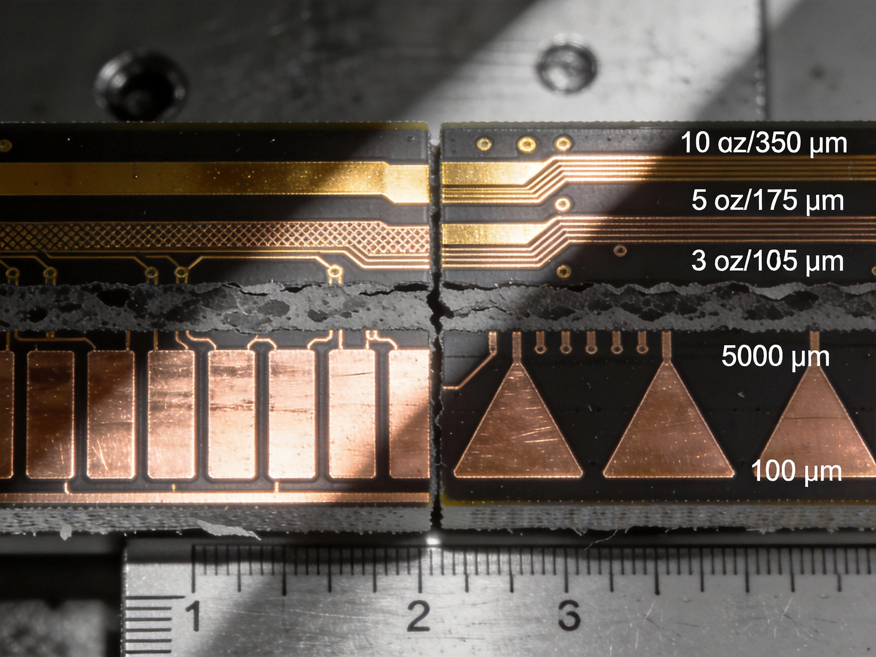
Copper Weight specifications describe the mass of copper per square foot of PCB surface area, expressed in ounces. Standard 1oz copper refers to one ounce of copper spread over one square foot, which produces approximately 1.37 mils (34.7 micrometers) of finished foil thickness after plating and processing. This terminology originates from the historical practice of measuring copper foil by weight, and it remains the industry standard despite the metric system's prevalence elsewhere.
When manufacturers specify 2oz copper, they target a finished Copper Thickness of approximately 2.74 mils (70 micrometers) on outer layers. Inner layer copper, which undergoes additional processing during lamination, may measure slightly thinner due to oxide treatment and laminate bonding effects. Understanding that specified weights refer to finished thickness—and accounting for the ~0.5oz to 1oz reduction from raw foil to finished conductor—prevents specification errors that could compromise current-carrying capacity.
The distinction between raw foil weight and finished weight matters most for controlled impedance designs and high-frequency applications. For Power Electronics where current capacity dominates considerations, the finished weight represents the relevant specification, and manufacturers adjust plating processes to achieve target thickness regardless of starting foil weight.
Standard PCB production utilizes 1oz copper almost universally, with processes, equipment, and material supply chains optimized around this weight. Moving to 2oz copper requires thicker raw foil stocks, modified plating chemistry to achieve uniform coverage in deeper features, and adjusted etching parameters to achieve Trace Geometry control despite longer etch times. These differences introduce cost at every production stage.
4oz copper represents a further escalation where manufacturing complexity increases non-linearly. The plating time required to add 3oz of copper (from 1oz base foil to 4oz finished) exceeds standard plating tank capacities for many facilities, requiring extended processing that reduces throughput. Trace Geometry control becomes more challenging as etchant must remove more copper, and undercut effects become proportionally more significant relative to target trace dimensions.
Copper raw material represents the most straightforward cost difference between 2oz and 4oz PCBs. Copper prices fluctuate with commodity markets, but the differential between 2oz and 4oz constructions typically ranges from $15 to $40 per square meter of board area. For a modest 100mm x 100mm board, this translates to approximately $0.15 to $0.40 in material cost difference—seemingly small in isolation but meaningful at production volumes.
Prepreg and laminate material costs remain relatively similar between constructions since substrate material requirements do not change with copper weight. However, Heavy Copper boards often require higher glass transition temperature (Tg) materials to withstand processing stress, which can add $2 to $8 per square meter depending on specification requirements. This material upgrade frequently accompanies heavy copper designs even when not strictly necessary, inflating costs when engineers specify unnecessarily high Tg ratings.
Surface Finish costs may increase for heavy copper boards depending on finish type. Enig (electroless nickel immersion gold) processing must deposit sufficient gold thickness to cover increased surface area from heavier topography. Immersion silver and OSP finishes scale more directly with surface area, adding proportionally to finish costs without the complexity of additional plating steps.
Etching time increases roughly proportionally with Copper Thickness, meaning 4oz boards require approximately twice the etch chemistry and chamber time compared to 2oz constructions. This extended processing reduces production throughput, effectively increasing labor overhead per board as fewer units flow through the production line per hour. Facilities typically recover this throughput reduction through higher pricing multipliers for heavy copper work.
Plating processes for 4oz copper outer layers require custom plating cycles that many standard PCB shops cannot accommodate without special scheduling. The additional copper deposition time—potentially three to four times standard cycle duration—forces heavy copper work into dedicated plating batches, adding setup overhead that amortizes across smaller production quantities. Some manufacturers charge 50% to 100% premiums specifically to recover plating capacity opportunity costs when scheduling heavy copper work.
Quality inspection for heavy copper boards requires additional attention compared to standard constructions. Trace geometry variations from non-uniform etching prove more consequential as the ratio of trace width tolerance to absolute trace width increases. A ±0.5 mil width tolerance on a 10mil trace represents 10% variation, but on a 40mil trace at 4oz copper it becomes only 2.5%—yet the absolute dollar cost of rejecting boards over this tolerance scales with the difficulty of meeting it.
Industry pricing data suggests the following approximate multipliers relative to standard 1oz copper baseline:
These multipliers vary significantly by manufacturer capability, geographic region, and order volume. High-volume production contracts often achieve better multipliers than small prototype quantities, and manufacturers specializing in heavy copper work generally offer more competitive pricing than general-purpose shops attempting occasional heavy copper jobs.
Determining whether 2oz copper provides adequate current-carrying capacity requires understanding both steady-state current requirements and transient thermal considerations. The Ipc-2152 standard provides guidance for conductor sizing based on temperature rise, though many engineers apply conservative multipliers that significantly overestimate actual requirements for their specific thermal environments.
For continuous currents below approximately 5 amps per millimeter of trace width with 2oz copper, the standard construction typically provides adequate margin. However, localized heating in high-current paths, uneven copper distribution creating thermal concentration, and poor thermal connectivity to ground planes can all degrade actual current capacity below theoretical calculations. A careful Thermal Analysis accounting for actual board mounting, adjacent component heating, and airflow conditions provides more reliable guidance than generic IPC charts alone.
The transition between 2oz and 4oz necessity typically occurs in the 5A to 15A continuous current range, depending on trace geometry, board Thermal Management, and acceptable temperature rise. Rather than defaulting to heavier copper to "be safe," engineers should perform quantitative analysis to determine whether 2oz provides sufficient margin or whether 4oz provides necessary performance improvement.
Heavier copper provides two thermal benefits beyond raw current capacity. First, lower electrical resistance reduces I²R heating proportional to the square of current, meaning 4oz copper dissipates one-quarter the heating of equivalent 1oz copper for the same current flow. Second, thicker copper spreads heat laterally more effectively through the plane, reducing localized hot spots that occur with narrow high-current traces.
For boards with excellent thermal connectivity to heatsinks or metal backings, the difference between 2oz and 4oz may be less significant than Thermal Analysis of isolated traces suggests. When copper planes bond directly to aluminum or copper substrates, current spreading through the plane reduces Current Density in individual traces, partially compensating for lighter copper weight. This effect proves particularly relevant for automotive and Power Electronics modules where metal-backed constructions are common.
Power electronics operating above 10-15A continuous current frequently justify 4oz copper construction based on thermal performance alone. Motor drives, inverters, battery management systems, and welding equipment commonly specify 4oz or heavier copper to manage junction temperatures in power semiconductors without excessive heatsinking. In these applications, the material cost premium typically represents a small fraction of overall system cost, while copper weight directly enables the thermal performance the application requires.
Automotive applications face particularly demanding requirements due to high ambient temperatures under-hood, Thermal Cycling from engine operation, and long warranty periods that demand robust thermal margins. Automotive Electronics standards often specify minimum copper weights regardless of calculated current requirements, providing conservative margin against field conditions that defy precise modeling. 4oz copper frequently appears in automotive power modules for these reasons.
High inrush current applications such as capacitive power supplies and pulsed laser drivers create transient thermal conditions where heavier copper provides margin against repetitive thermal stress. Even when average current falls within 2oz capability, peak currents may exceed the thermal capacity of lighter copper, causing cumulative damage over thousands of operating cycles.
Beyond electrical requirements, 4oz copper offers manufacturing benefits that can offset some of its cost premium. Thicker copper provides greater mechanical strength for connectors and terminals that undergo repeated mating cycles. The robust conductor cross-section resists fatigue cracking from Thermal Cycling better than lighter alternatives, potentially improving Field Reliability for applications with demanding environmental exposure.
Heavier copper enables lower-impedance ground returns and Power Distribution networks that reduce noise coupling in mixed-signal electronics. While this benefit primarily applies to specialized applications, it can justify 4oz specification when signal integrity requirements drive board design rather than pure power handling considerations.
Many designs unnecessarily specify heavy copper for the entire board when only specific regions carry High Current. Strategic specification of 2oz base copper with selective plating-up of 4oz features in current-carrying zones can reduce material costs while achieving necessary performance. This approach requires careful coordination with the manufacturer to ensure plating thickness control in targeted areas.
Coin insertion techniques embed solid copper blocks directly into the PCB stackup for extreme current applications, replacing plated copper with machined copper that provides superior current capacity and thermal conductivity. While adding assembly complexity, coin insertion can reduce total copper cost for applications requiring very heavy copper in limited areas, particularly when combined with standard construction elsewhere on the board.
Trace geometry optimization reduces copper weight requirements by maximizing current capacity per unit width. Wider traces at lighter copper weights sometimes provide equivalent current capacity to narrower traces with heavier copper, at lower total material cost. A 20mil wide trace at 4oz carries similar current to a 40mil trace at 2oz, but the wider trace consumes more board area—trade-offs that favor one approach or the other depending on layout density requirements.
Copper Pour and plane fill strategies maximize current-carrying capacity while minimizing actual copper usage. Thermal relief connections between planes and pads prevent Solder Wicking during assembly while providing robust electrical connection. Proper plane geometry ensures Current Distribution through the plane rather than concentrating in narrow neck-down regions that require heavier copper to handle Current Density.
Not all PCB manufacturers handle heavy copper equally well, and capability significantly affects pricing competitiveness. Shops with dedicated heavy copper plating lines and established processes for thick copper processing typically offer better pricing than general-purpose manufacturers adding heavy copper to their standard menu as an afterthought. The difference can exceed 30% for comparable quality, making supplier selection a critical cost optimization lever.
Prototype and low-volume orders face the steepest pricing relative to standard construction because fixed setup costs amortize across fewer units. Consolidating heavy copper work into periodic production runs rather than frequent small orders improves pricing through better fixed-cost amortization. Some manufacturers offer prototype pricing specifically designed to make initial qualification more accessible, then apply standard production pricing for subsequent high-volume orders.
A 100mm × 100mm four-layer PCB with 2oz copper on power and ground layers and standard 1oz on signal layers might quote at $25 to $40 per board for 100-piece production, compared to $55 to $90 per board for equivalent 4oz construction. The $30 to $50 per board premium represents approximately 2x cost increase for 2x copper weight, illustrating that the relationship between copper weight and cost is not strictly linear.
If only 30% of board area carries High Current requiring 4oz specification, selective heavy copper placement might reduce the effective premium to $10 to $20 per board, achieving necessary performance at approximately 50% of full-4oz pricing. This optimization approach works best when high-current zones occupy predictable regions of the board layout.
A larger 150mm × 200mm six-layer automotive power module requiring all layers at 4oz copper might quote at $180 to $280 per board for 50-piece production. The same board at 2oz construction might price at $75 to $110 per board—a significant difference that forces careful evaluation of whether 2oz provides adequate margin for the automotive operating environment.
When the application requires AEC-Q100 or similar automotive qualification, the manufacturing cost premium often proves worthwhile against the cost of field returns and warranty exposure. Automotive manufacturers frequently specify conservative copper weights specifically to ensure margin against conditions more severe than design assumptions, accepting higher material costs to reduce lifetime reliability risk.
The cost comparison between 2oz and 4oz copper PCBs reveals that pricing does not scale linearly with copper weight—manufacturing complexity increases disproportionately, with typical 4oz costs running 2x to 3x equivalent 2oz boards. This premium demands thoughtful evaluation of whether heavier copper genuinely provides necessary performance improvement or whether 2oz with optimized geometry achieves the same result at lower cost.
For applications below 5A continuous current with good Thermal Management, 2oz copper typically provides generous margin and represents the cost-optimal choice. For higher current applications, automotive requirements, or designs with demanding thermal environments, 4oz copper frequently justifies its premium through improved thermal performance and reliability margin.
Selective heavy copper placement, design optimization, and strategic supplier selection all offer opportunities to manage costs while achieving necessary performance. Engaging manufacturing partners early in the design process to review copper weight specifications and explore optimization options frequently reduces costs more effectively than value engineering efforts applied after designs are finalized.
4oz copper PCBs typically cost 2x to 3x equivalent 1oz construction in production quantities. The premium varies by manufacturer capability, order volume, and board complexity. Prototype quantities face even higher multipliers due to fixed setup costs amortizing across fewer boards.
Whether 2oz copper suffices depends on specific current levels, thermal environment, and acceptable temperature rise. For continuous currents below 10A in typical conditions with reasonable thermal management, 2oz often provides adequate capacity. Higher currents or elevated temperatures may require 4oz or heavier construction to maintain acceptable junction temperatures.
Manufacturing complexity increases disproportionately with copper weight. Plating time, etch time, and process control requirements all scale non-linearly, and many facilities handle heavy copper work as specialty production that commands premium pricing to recover opportunity costs of reduced throughput.
Heavy Copper Pcb production typically adds 5 to 10 business days to standard lead times due to extended plating and processing cycles. Manufacturers with dedicated heavy copper capabilities may offer shorter incremental lead times compared to shops adding heavy copper to standard production lines.
No. Heavy copper manufacturing requires specific plating tank capacity, process expertise, and quality control capabilities that not all manufacturers possess. Attempting heavy copper work at facilities without appropriate capability often results in quality problems that exceed any pricing advantage, making supplier selection critical for heavy copper projects.
High Current PCB Layer Stackup: Symmetrical vs. Asymmetrical Power PlanesJuly/20/2026
High Current PCB Embedded Copper: Internal vs. External Heat DissipationSeptember/26/2026
High Current PCB Mounting Holes: Plated vs. Non-Plated for Current ReturnSeptember/29/2026
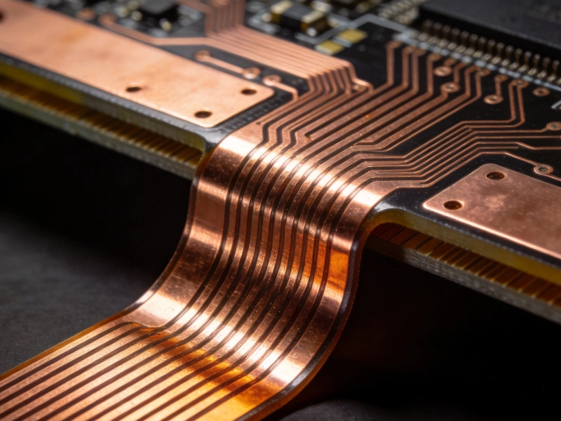
High Current PCB Flex-Rigid: Current Capacity in Bend AreasOctober/09/2026
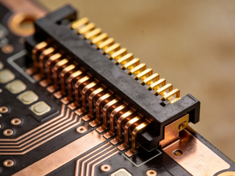
High Current PCB Edge Connectors: Current Rating and Thermal LimitsSeptember/20/2026
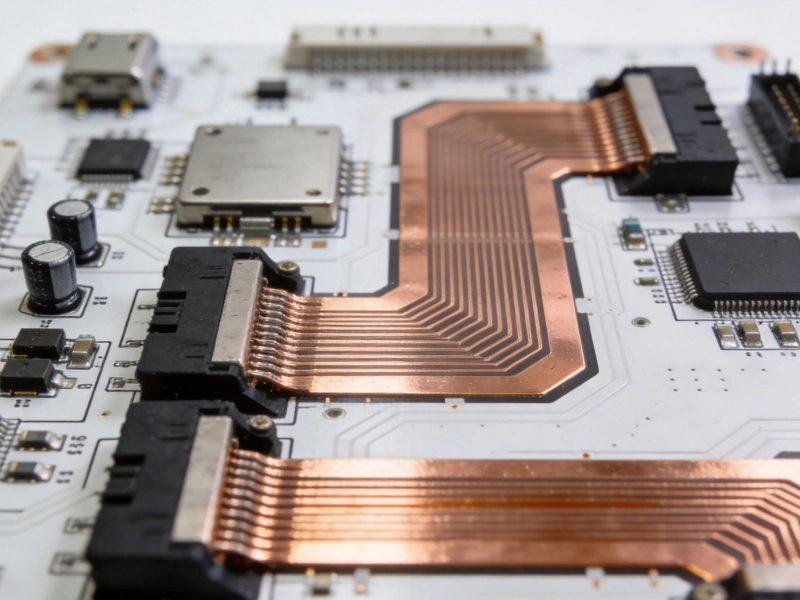
High Current PCB Design for Aerospace Power DistributionSeptember/08/2026
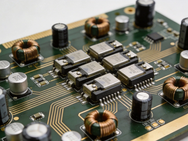
High Current PCB Design for Audio Amplifiers: Avoiding Ground LoopsSeptember/14/2026
Copper Pour vs Trace: What 3 Years of PCB Failures Taught UsMay/21/2026