

Every PCB generates heat when current flows through its traces. At low current levels—tens or hundreds of milliamps—the heat is negligible, dissipated quickly by the surrounding material, and rarely a concern. But when current climbs into the ampere range and beyond, the story changes dramatically. A standard 1-ounce Copper Trace carrying 5 amperes can reach temperatures that are uncomfortable for the board and its surrounding components. At 10 or 15 amperes, a standard PCB may exceed safe operating temperatures, causing solder joint degradation, component damage, and premature board failure. This is the problem that High Current PCBs are designed to solve, and in this article, we put them head-to-head against standard boards in a real-world thermal stress test.
Understanding how High Current PCBs and standard PCBs behave under thermal stress is essential for anyone designing Power Electronics, motor controllers, battery management systems, Led Drivers, or any application where significant current must be routed through the board. This article presents a practical comparison based on thermal imaging, temperature measurements, and analysis of how each board type handles the heat generated by sustained current flow.
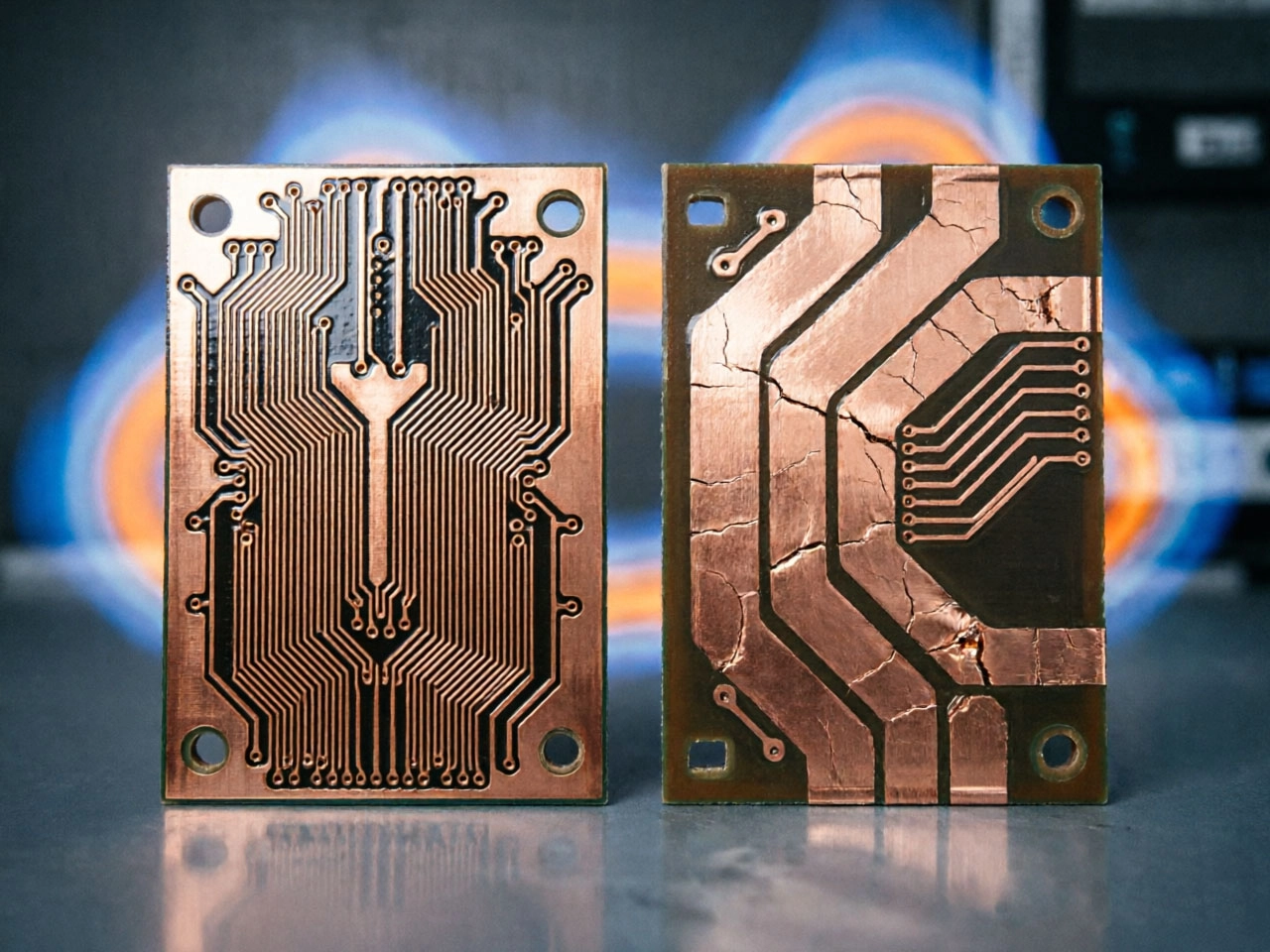
Before diving into the test results, it helps to understand why current flowing through a Copper Trace generates heat in the first place. The answer lies in the basic physics of electrical resistance.
Copper is not a perfect conductor. It has a finite electrical resistance that depends on the trace's cross-sectional area, length, and temperature. When current flows through this resistance, electrical energy is converted to thermal energy—a phenomenon described by Joule's first law, which states that the power dissipated as heat equals the current squared multiplied by the resistance. This relationship has a critical implication: doubling the current quadruples the heat generated, because the current term is squared. A trace carrying 10 amperes generates four times as much heat as one carrying 5 amperes, not twice as much.
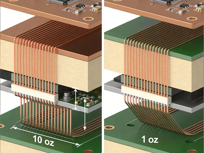
The cross-sectional area of the copper trace determines its current-carrying capacity and its ability to dissipate the heat it generates. A wider and thicker trace has more cross-sectional area, lower resistance per unit length, and a larger surface area from which heat can be radiated and convected away. Standard PCBs with 1-ounce copper (approximately 1.4 mils or 35 micrometers thick) and trace widths in the range of 0.2 to 0.5 millimeters are designed for signal routing and low-Power Distribution, not high-current delivery. High current PCBs use thicker copper—2 ounces, 3 ounces, or even 6 ounces or more—and wider traces specifically to handle ampere-level currents with acceptable temperature rise.
To provide a fair and meaningful comparison, we designed two versions of the same simple Power Distribution circuit: a 4-layer board with a main power bus distributing current from an input connector to multiple output loads. The only differences between the two boards were the Copper Weight and trace widths on the current-carrying bus bars. Both boards used the same dielectric material (standard FR-4, Tg 140), the same board thickness (1.6 millimeters), and the same surface mount components at the same locations.
The standard board used 1-ounce copper on all layers, with power bus traces sized at 3 millimeters wide on the outer layers and 3-millimeter-wide planes on the inner layers. The high current board used 3-ounce copper on the outer layers and 2-ounce copper on the inner layers, with Bus Bar widths increased to 6 millimeters on the outer layers and corresponding inner plane areas. Both boards were fabricated by the same manufacturer using the same process parameters where applicable.
Each board was powered up and subjected to a stepped current loading test, starting at 1 ampere and increasing in 1-ampere increments until reaching 12 amperes. At each current level, we waited 10 minutes for the board to reach thermal equilibrium, then captured thermal images using a FLIR thermal camera and recorded the temperature at multiple points on the board using thermocouple probes. We also monitored the temperature of key components, including the input connector, the main bus traces, and the output load resistors.
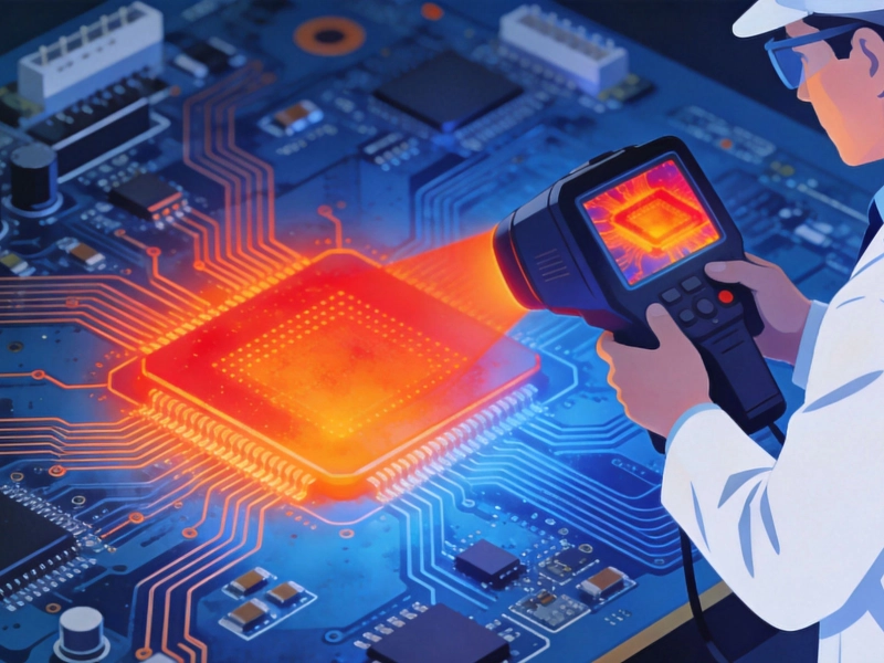
The thermal images told the story more clearly than any number could. On the standard PCB, visible heating began at around 2 amperes, with the main power bus showing a warm glow compared to the surrounding board area. At 5 amperes, the bus trace was noticeably hot, with temperatures climbing above 60 degrees Celsius in some areas. At 8 amperes, the board showed significant thermal stress, with the hottest points approaching 85 degrees Celsius and visible discoloration beginning to appear on the solder mask near the input connector. By 10 amperes, the board was running at temperatures that would be concerning in a production environment, with the hottest areas approaching 100 degrees Celsius.
The High Current PCB told a dramatically different story. At 2 amperes, the board showed essentially no measurable temperature rise over ambient. Even at 5 amperes, the thermal camera showed only a faint warmth on the power bus traces, with maximum temperatures around 35 degrees Celsius above ambient—a comfortable margin below any concern threshold. At 8 amperes, the high current board showed moderate warming, with the hottest points reaching approximately 45 degrees Celsius above ambient. At 10 and 12 amperes, the board was warm but well within safe operating limits, with maximum temperatures staying below 65 degrees Celsius even at the highest current levels tested.
The comparison is stark: at 10 amperes, the standard PCB was approaching temperatures that would degrade solder joints and shorten component life, while the High Current PCB was running comfortably cool. The difference is entirely attributable to the larger copper cross-section and wider traces on the high current board, which provide lower resistance and better heat spreading.
Beyond the visual thermal imaging, the thermocouple measurements provide quantitative data that confirms the observations. The following patterns emerged from the temperature measurements across both boards.
At low current levels (1 to 3 amperes), both boards performed adequately, with temperature rises of less than 15 degrees Celsius above ambient on the standard board and essentially negligible rises on the high current board. For applications operating in this current range, a well-designed standard PCB can handle the thermal load without issue.
Between 4 and 6 amperes, the divergence became pronounced. The standard board showed temperature rises in the 25 to 45 degrees Celsius range, which is acceptable for short-term operation but would be concerning for continuous duty in enclosed equipment. The high current board showed rises of only 10 to 20 degrees Celsius in this range—well within safe operating parameters.
Above 6 amperes, the standard board entered problematic territory. Temperature rises of 50 to 65 degrees Celsius above ambient mean that in a 25-degree Celsius room, the board surface reaches 75 to 90 degrees Celsius—hot enough to soften solder, accelerate electromigration, and reduce the lifespan of semiconductors and connectors. The high current board maintained temperature rises of 25 to 40 degrees Celsius in this range, keeping the board surface below 65 degrees Celsius even at 12 amperes.
One interesting observation was that the temperature rise was not uniform across the board in either case. The hottest points on both boards were always near the input connector, where Current Density is highest before the bus spreads the current across the wider trace network. This highlights the importance of generous landing pad sizes and wide trace transitions at current entry points—a design principle that applies to both standard and high current PCBs but is especially critical on standard boards where thermal margins are smaller.
The thermal struggles of standard PCBs under high current are not a quality defect—they are a fundamental consequence of the design trade-offs that make standard PCBs excellent for their intended purpose: signal routing and low-power distribution. Standard PCBs are optimized for routing density, cost efficiency, and compatibility with fine-pitch components. The thin copper and relatively narrow traces that enable fine-pitch routing also create high resistance paths for current, which generates excessive heat at ampere-level currents.
The 1-ounce Copper Weight used on standard PCBs provides approximately 35 micrometers of Copper Thickness. For a 3-millimeter-wide trace, this gives a cross-sectional area of approximately 0.105 square millimeters. The resistance of such a trace carrying 10 amperes generates approximately 2.3 watts per centimeter of trace length—enough to create significant heating even in a short trace. By comparison, a 6-millimeter-wide trace with 3-ounce copper (approximately 105 micrometers thick) provides a cross-sectional area of 0.63 square millimeters—six times greater—which reduces resistance by a factor of six and heat generation by a factor of six for the same Current Density per unit width.
Standard PCBs also suffer from thermal spreading limitations. The heat generated in a thin copper trace must conduct through the thin trace material and then through the dielectric substrate before it can spread laterally. The thermal conductivity of FR-4 is relatively poor (approximately 0.29 W/m·K), which means heat spreads slowly sideways from a narrow trace. A wider, thicker trace on a High Current Pcb spreads heat more effectively because it has more surface area in contact with the board and more volume from which heat can dissipate.
High current PCBs are purpose-built for power applications, and their design advantages reflect the specific requirements of routing significant current safely and reliably.
Increasing copper weight from 1 ounce to 2, 3, or 4 ounces dramatically reduces the resistance of current-carrying traces. The relationship is approximately linear: doubling the copper weight halves the resistance, which halves the heat generated for the same current. For applications that must carry 10 amperes or more on a single trace, this reduction in resistance is transformative. It is worth noting that increasing copper weight does increase cost and requires adjustments to the assembly process (longer reflow times due to higher thermal mass), but for the power portion of the board, these trade-offs are well worth it.
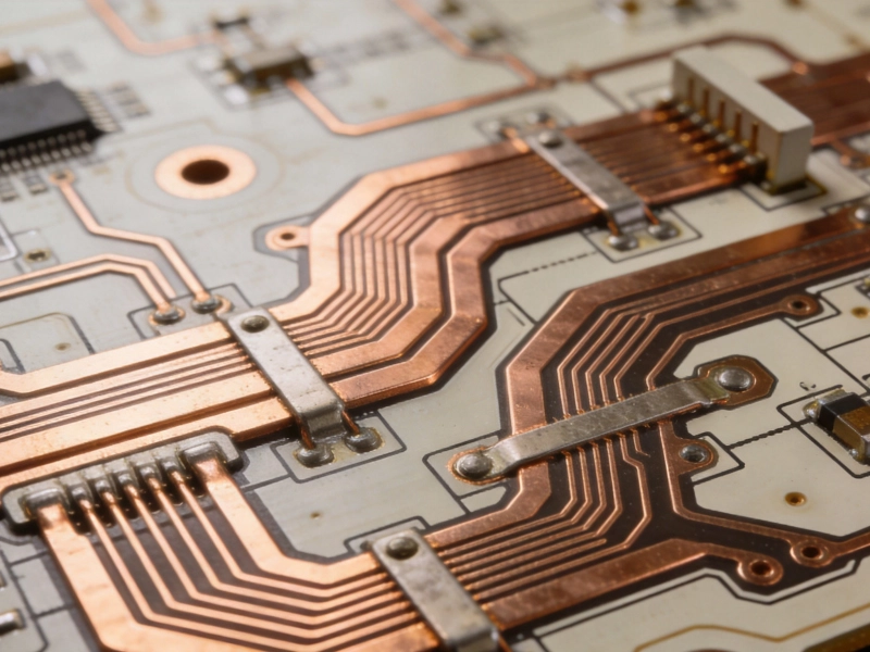
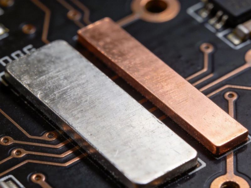
High current PCBs typically use wider traces or dedicated power plane areas rather than routing current through narrow signal-style traces. A power Bus Bar—a wide strip of copper running across the board—provides a low-resistance path for current with excellent heat spreading characteristics. The wide surface area of a bus bar allows heat to dissipate efficiently into the surrounding environment, keeping temperatures low even under sustained high-current operation. Some high current designs use exposed copper bus bars without solder mask, which further improves Heat Dissipation through radiation and convection.
For multilayer high current boards, Thermal Vias connecting the current-carrying layers to inner ground planes or dedicated thermal planes can significantly improve heat spreading. A thermal via array placed beneath a high-power component or along a high-current bus helps conduct heat away from the hot spot and distribute it across a larger area of the board. The key is using an adequate number and density of vias—typically at least 9 to 16 vias per square centimeter in the thermal path—to ensure low Thermal Resistance through the via array.
High Current Pcb Design is not just about the board itself—the components must also be rated for the current levels involved. Input and output connectors must have current ratings well above the maximum operating current, with generous terminal sizes that can handle the current density without excessive heating. MOSFETs and other power semiconductors must have sufficiently low on-resistance (Rds-on) to minimize internal heat generation. Current sense resistors must be rated for the expected power dissipation, which is equal to the current squared multiplied by the sense resistance. Selecting components with adequate thermal margins ensures that the system as a whole stays within safe operating limits.
If your design involves currents above approximately 3 amperes per trace, the following guidelines will help you create a High Current Pcb that performs reliably.
Despite the clear thermal advantages of high current PCBs, there are situations where a standard PCB is still the appropriate choice, and forcing a High Current Design where it is not needed adds unnecessary cost and complexity.
For applications where maximum current per trace stays below approximately 2 to 3 amperes, a well-designed standard PCB with appropriately sized traces is perfectly adequate. A digital control board with multiple ICs drawing a few hundred milliamps each, for example, distributes current through many parallel paths, none of which carries enough current to create significant heating on a standard trace. In these cases, using standard PCB specifications keeps cost low and manufacturing straightforward.
Additionally, high current PCB features like heavier copper and wider traces are incompatible with fine-pitch component routing. If your board mixes high-current sections with fine-pitch digital components, the best approach is a hybrid design: dedicated Power Planes and wide bus bars for current delivery, combined with standard routing density for signal traces. Designing these as separate areas of the board, with clear demarcation in the layout, makes the manufacturing and assembly process more straightforward.
There is no single answer, as safe Current Carrying Capacity depends on trace width, trace length, ambient temperature, airflow, and the acceptable temperature rise. As a rough general guideline using external trace width calculators, a 1-millimeter-wide trace on a standard 1.6-millimeter FR-4 board in still air can carry approximately 1 to 1.5 amperes with a 10 to 20 degree Celsius temperature rise. Wider traces and lower temperature rise requirements reduce this value proportionally. Always use a current density calculator or thermal simulation tool for your specific conditions rather than relying on general estimates.
High current PCB Fabrication costs more than standard PCB primarily because of the heavier copper weight. The raw material cost of 3-ounce copper is approximately 2.5 to 3 times the cost of 1-ounce copper. Additionally, the wider traces and bus bars on high current boards consume more panel area, which reduces the number of boards per panel and increases per-board cost. As a rough estimate, a high current PCB with 3-ounce copper and wide bus bars costs approximately 40 to 60 percent more than an equivalent standard board. For applications where the board carries 5 amperes or more continuously, this cost premium is justified by the reliability improvement.
Adding bus bars or copper foil to an existing board after fabrication is not practical or reliable. The copper must be laminated during the board manufacturing process to achieve proper adhesion and electrical connection. After-market additions using conductive epoxy or soldered-on copper strips do not provide reliable electrical or thermal performance. If you need higher current capacity than originally designed, the best solution is to re-fabricate the board with heavier copper weight and wider traces from the start.
Thermal Vias conduct heat from a component or trace through the board's dielectric layers to inner ground planes or thermal planes, which act as heat spreaders. A thermal via under a hot component can reduce its junction temperature by 10 to 20 degrees Celsius or more by spreading the heat across a larger area of the board. For maximum effect, thermal vias should be placed directly under the heat source, be of adequate diameter (typically 0.3 to 0.5 millimeters), and have thin barrel walls to maximize copper cross-section and thermal conductivity.
Yes. Elevated temperatures caused by high current accelerate multiple failure mechanisms, including solder joint fatigue from Thermal Cycling, electromigration of copper atoms in high-current-density areas, degradation of dielectric materials, and increased failure rates of semiconductor components. Boards that run at temperatures below 80 degrees Celsius under continuous operation typically have acceptable long-term reliability. Boards running above 100 degrees Celsius experience significantly accelerated aging and should be designed with larger thermal margins or active cooling solutions.
The thermal stress test results leave little room for ambiguity. Standard PCBs, designed for signal routing and low-power distribution, are fundamentally unsuited for sustained high-current operation above approximately 3 to 5 amperes per trace without significant Thermal Management measures. Their thin copper and narrow traces create resistance levels that generate excessive heat, leading to temperatures that degrade reliability and shorten component life.
High current PCBs, purpose-built with heavier copper, wider traces, and bus bar topologies, handle ampere-level currents with ease. In our test, a high current board carrying 10 amperes stayed cooler than a standard board carrying 5 amperes. This performance advantage translates directly into improved reliability, longer service life, and broader safe operating margins.
For engineers designing Power Electronics, motor controllers, battery management systems, Led Drivers, or any application where current levels exceed a few amperes, the message is clear: invest in High Current Pcb Design from the beginning. The incremental cost of heavier copper and wider traces is small compared to the cost of field failures, warranty repairs, and customer dissatisfaction caused by boards that run too hot. Designing for thermal margin from the start is always cheaper than redesigning after a thermal failure.
This article is provided for general informational purposes regarding high current Pcb Design and thermal performance. Actual test results and thermal behavior will vary based on specific board designs, materials, environmental conditions, and manufacturing parameters. Always verify thermal performance through simulation and physical testing for your specific application.
Building a High Current PCB Power Supply for Server RacksJuly/30/2026
Building a 50A DC-DC Converter: High Current PCB Layout Lessons LearnedJuly/12/2026
Copper Pour vs Trace: What 3 Years of PCB Failures Taught UsMay/21/2026
Heavy Copper vs Standard Copper PCB: Complete Comparison Guide for EngineersMay/20/2026
High Current PCB Daisy-Chain vs. Star Routing: Voltage Drop ComparisonAugust/08/2026
Plated Through Hole Current Rating: Complete Guide for PCB DesignersMay/21/2026
5 Critical Thermal Management Problems in High Power PCBsMay/21/2026
High Current PCB Pad Design: Reinforced Plating vs. Standard PadsJuly/28/2026