
Designing printed circuit boards that safely handle high currents while maintaining reliability requires more than guesswork and rule-of-thumb estimates. The Ipc-2152 standard provides the definitive methodology for determining current-carrying capacity in Pcb Design, replacing outdated approaches with scientifically validated calculations. Whether you are designing power supplies, motor controllers, or high-Current Distribution systems, understanding Ipc-2152 ensures your traces carry current safely without overheating, voltage drop issues, or premature failure.
IPC-2152, titled "Standard for Determining Current-Carrying Capacity in Printed Board Design," represents the authoritative industry guideline for calculating how much current PCB conductors can safely carry. Published by IPC, the association connecting electronics industries, this standard supersedes the older Ipc-2221 approach with more accurate modeling based on extensive empirical testing.
The key insight from IPC-2152 is that Trace Current Capacity is not determined by a single chart or simple formula. Instead, it depends on a complex interplay of factors including trace dimensions, Copper Thickness, temperature rise, layer position, surrounding environment, and thermal coupling from adjacent conductors. Understanding these variables enables engineers to optimize PCB designs for both safety and space efficiency.
At its heart, IPC-2152 provides both graphical nomographs and mathematical approximations for calculating Trace Current Capacity. The fundamental equation relates current, temperature rise, and cross-sectional area:
I = k × ΔT^0.44 × A^0.725
Where:
The cross-sectional area depends on trace width and Copper Thickness:
A = Width × Copper Thickness
For copper thickness, remember these standard conversions:
The correction factor k differs significantly between outer and inner layers due to thermal dissipation differences:
This means outer layer traces can carry approximately twice the current of inner layer traces with the same dimensions, because heat dissipates more effectively when one side is exposed to air.
The allowable temperature rise is perhaps the most critical design parameter. Common choices include:
Remember that the final trace temperature equals ambient temperature plus ΔT. A trace with ΔT = 20°C in a 40°C environment reaches 60°C, which may exceed material limits.
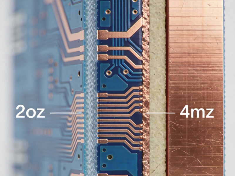
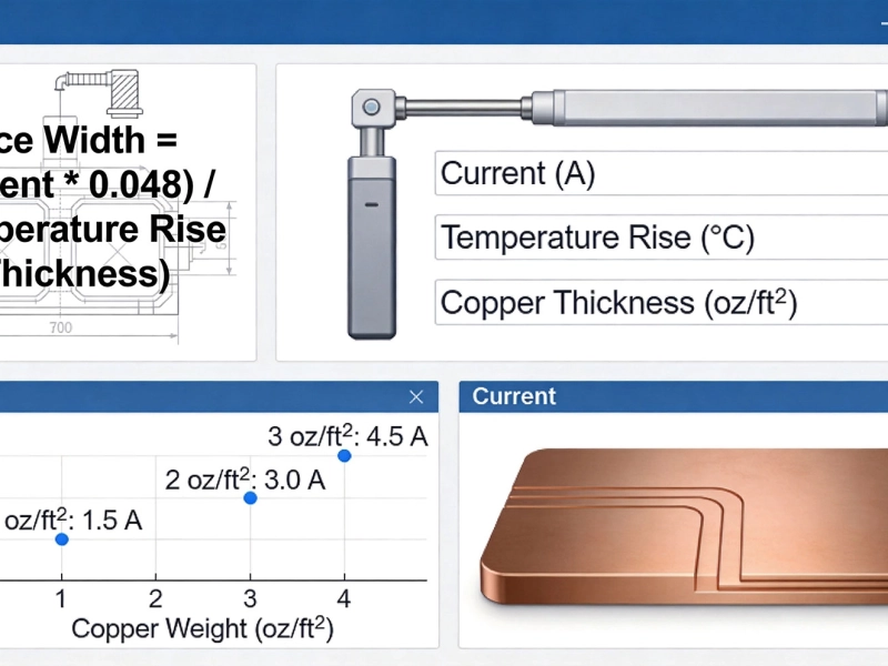
Copper Weight directly impacts current capacity through increased cross-sectional area. Increasing from 1 oz to 2 oz approximately doubles current capacity, enabling narrower traces for the same current or higher currents for the same width.
Common Copper Weight options:
Width is the primary design variable you control. Wider traces provide more cross-sectional area, reducing resistance and heat generation. However, excessive width wastes board space, so accurate calculation optimizes the balance between safety and efficiency.
As mentioned, layer position significantly affects thermal performance:
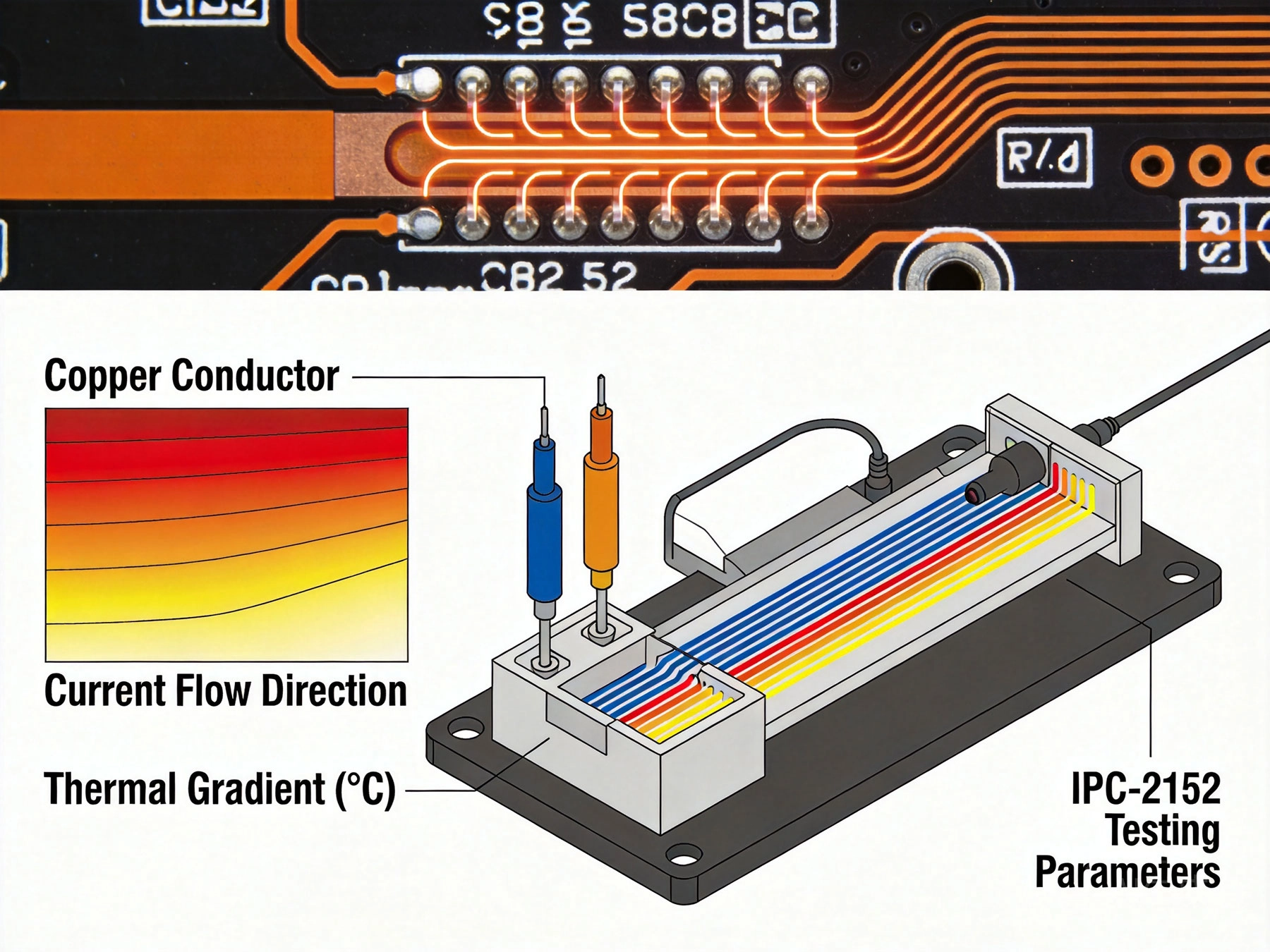
IPC-2152 introduced an important consideration largely ignored by earlier standards: nearby conductors carrying current generate thermal coupling effects. Dense high-current bus bars can heat each other, raising actual temperatures above calculations based on isolated traces. Design spacing between high-current traces of at least 3 times the trace width when possible.
Different substrate materials have varying thermal conductivity, affecting Heat Dissipation:
Consider the actual operating environment:
| Current (A) | Width (mm) at ΔT=10°C | Width (mm) at ΔT=20°C | Width (mm) at ΔT=30°C |
|---|---|---|---|
| 1 | 0.30 | 0.20 | 0.15 |
| 2 | 0.60 | 0.40 | 0.30 |
| 3 | 0.90 | 0.60 | 0.45 |
| 5 | 1.50 | 1.00 | 0.75 |
| 10 | 3.20 | 2.10 | 1.60 |
| Current (A) | Width (mm) at ΔT=10°C | Width (mm) at ΔT=20°C | Width (mm) at ΔT=30°C |
|---|---|---|---|
| 1 | 0.60 | 0.40 | 0.30 |
| 2 | 1.20 | 0.80 | 0.60 |
| 3 | 1.80 | 1.20 | 0.90 |
| 5 | 3.00 | 2.00 | 1.50 |
| 10 | 6.40 | 4.20 | 3.20 |
Note: Inner layer traces require approximately 1.5-2 times the width of outer layer traces for equivalent current capacity.
Design a power trace on an outer layer carrying 3A with ΔT = 20°C using 1 oz copper.
Step 1: Calculate required cross-sectional area using the formula rearranged:
A = [I / (k × ΔT^0.44)]^(1/0.725)
Step 2: Substitute values:
A = [3 / (0.048 × 20^0.44)]^(1/0.725)
A = [3 / (0.048 × 3.56)]^(1.38)
A = [3 / 0.171]^(1.38)
A = 17.5^1.38
A ≈ 67.5 mil²
Step 3: Calculate required width:
Width = A / Copper Thickness
Width = 67.5 / 1.37 ≈ 49 mil ≈ 1.25 mm
With safety margin (20%): Width ≈ 1.5 mm
Through-hole vias often become current bottlenecks in PCB designs. Unlike traces, vias have annular ring cross-sections, making their current capacity more complex to calculate.
General guidelines for standard vias:
For higher currents, use multiple parallel vias or Thermal Vias connected to large copper planes. Always verify via capacity with your specific manufacturing specifications.
The industry-standard free tool for IPC-2152 calculations. Features include:
Modern Pcb Design software includes current-carrying capacity features:
Several websites offer convenient IPC-2152 calculators:
When frequencies exceed approximately 10 MHz, skin effect becomes significant. Current flows primarily near the conductor surface, reducing effective cross-sectional area and increasing effective resistance.
Skin depth calculation:
δ = 66 / √f (mm) where f is frequency in Hz
For example, at 100 kHz, skin depth is approximately 0.2 mm. For high-frequency designs, consider:
Always include design margins to account for uncertainties:
Always verify critical high-current designs through:
IPC-2152 represents a significant advancement over the older Ipc-2221 Standard:
Designing each trace independently without considering heat from neighboring high-current conductors leads to cumulative overheating.
While "1mm per Amp" is a useful mnemonic, it ignores critical factors like temperature rise, copper weight, and layer position that dramatically affect requirements.
Using single vias for high-current paths is a common failure point. Always verify via capacity or use multiple parallel vias.
A ΔT of 20°C is acceptable in a 25°C room but dangerous in a 70°C industrial enclosure. Always consider the actual operating environment.
Copper plating is rarely perfectly uniform. Real-world traces may have thinner areas that limit current capacity. Use conservative calculations or specify your manufacturer's minimum tolerances.
IPC-2152 is the newer, more accurate standard that considers thermal coupling between traces, PCB material properties, and board thickness. Ipc-2221 provided simpler charts that often led to overly conservative or inaccurate designs. IPC-2152 typically allows more optimized designs when all factors are properly considered.
Use the formula I = k × ΔT^0.44 × A^0.725 with appropriate values for your layer position and copper weight. Alternatively, use Saturn PCB Toolkit or your EDA software's built-in calculator for IPC-2152 compliant results.
Yes, forced air cooling, Thermal Vias to Heat Sinks, or metal-core PCBs can increase effective current capacity. However, verify your specific cooling implementation matches the assumptions in your calculation method.
A minimum of 20% above calculated requirements is recommended for most applications. High-reliability or harsh environment designs may warrant 30-50% margins to account for manufacturing variations and unexpected conditions.
Approximately, yes. Inner layer traces cannot dissipate heat as effectively since both sides are constrained by dielectric material. The factor varies from about 1.5x to 2x depending on specific conditions, but designing with this assumption ensures reliable operation.
The IPC-2152 formula applies to continuous DC currents. For pulsed currents, the heating effect depends on duty cycle and pulse width. Short pulses with sufficient cooling time between them can carry higher peak currents. Consult detailed Thermal Analysis or testing for pulse applications.
Accurate current-carrying capacity calculation using IPC-2152 is essential for designing reliable PCBs that handle required currents without overheating or failing. The standard provides a scientifically grounded methodology that accounts for the complex thermal dynamics affecting trace current capacity.
Key takeaways for implementing IPC-2152 in your designs:
By moving beyond rule-of-thumb estimates to proper IPC-2152 calculations, you can optimize your PCB designs for both safety and efficiency, avoiding both the waste of excessive trace widths and the hazards of undersized conductors.

High Current PCB Thermal Relief: Full Connect vs. Modified SpokesJuly/16/2026
2oz vs. 4oz Copper: Which is Best for Your High Current PCB?July/10/2026
High Current PCB Trace Width Calculator: The Ultimate Engineering GuideMay/20/2026
Designing a High Current PCB Motor Driver: Avoiding EMI PitfallsJuly/14/2026
Designing a 100A High Current PCB for EV Battery Management SystemsJuly/09/2026
High Current PCB Design Guidelines: Ensuring Reliability and SafetyJune/08/2026
Why Your High-Power PCBs Overheat (And the 5 Methods That Actually Fix It)May/20/2026

5 Critical Thermal Management Problems in High Power PCBsMay/21/2026