
Every electronics engineer faces this moment: your power-hungry application needs to move serious current—tens or even hundreds of amps—but your Pcb Traces just aren't cutting it. You start doing the math and realize you'd need a trace wider than your entire board to safely carry the current without turning your design into a space heater.
This is where the debate between bus bar vs PCB trace for High Current applications becomes critical. Both solutions have their place in Power Electronics, and picking the wrong one can mean the difference between a reliable product and one that fails spectacularly in the field. After working on power distribution systems for electric vehicles, industrial drives, and server power supplies, I've learned the ins and outs of when each approach makes sense.
Let's break down this High Current showdown and help you make the right choice for your next project.
Pcb Traces are the traditional workhorses of current distribution on circuit boards. The copper箔 on your PCB forms conductive paths that carry signals and power throughout your design. For low to moderate currents—think anything under 10-20 amps—standard traces work just fine with proper width and thickness selection.
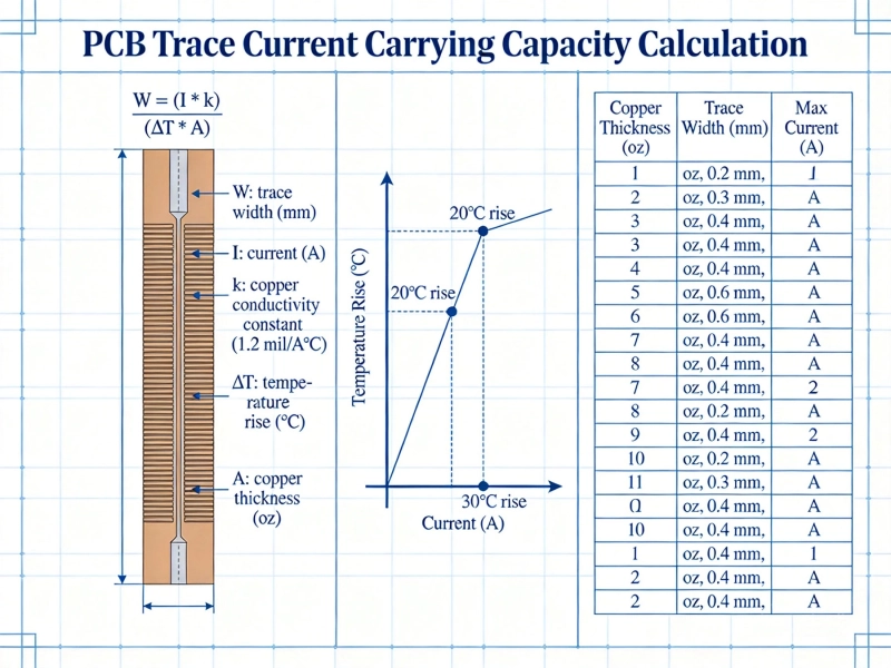
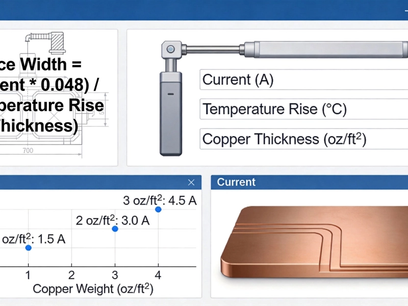
The fundamental relationship is straightforward: Current Carrying Capacity depends on cross-sectional area. Wider traces and thicker copper箔 mean more current can flow without excessive temperature rise. The IPC standards provide formulas and tables for calculating minimum trace width based on:
Here's where things get tricky. When you need to move 50, 100, or 200+ amps, the trace requirements become impractical:
These limitations don't mean PCB traces are bad—they're excellent for their intended purpose. But for true high current applications, you often need to think beyond the board itself.
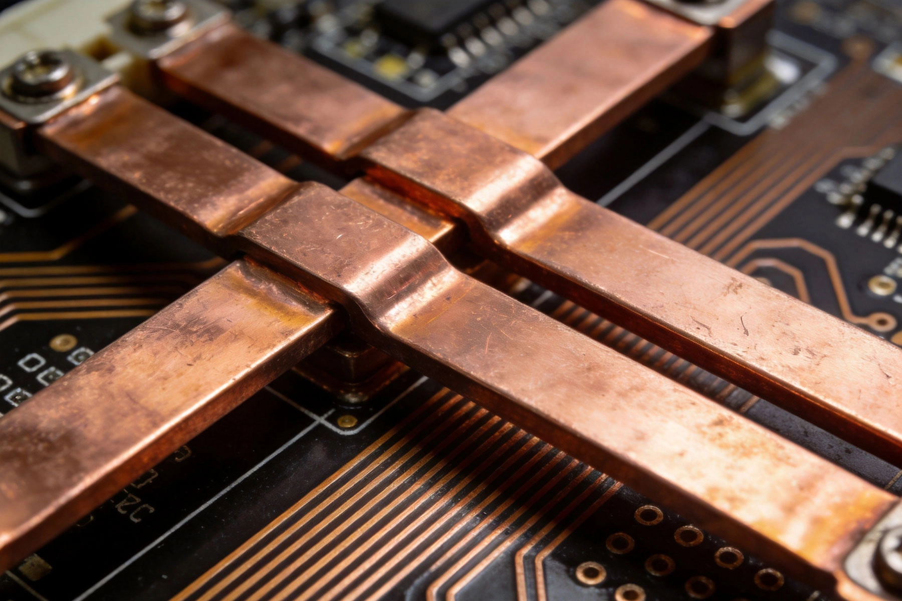
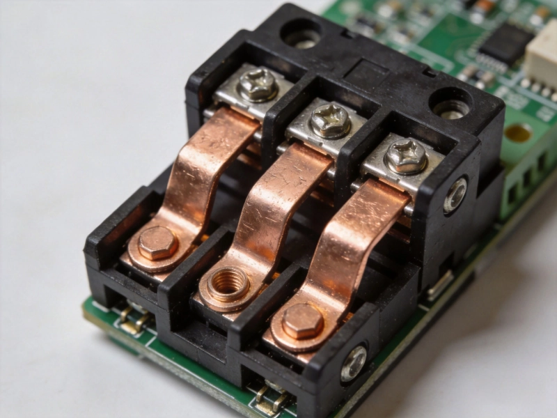
A bus bar is a solid metal conductor—typically copper or aluminum—designed to carry substantial currents between circuit sections or system components. Unlike PCB traces that are etched from copper箔, bus bars are separate pieces of metal that get connected to your board through soldering,bolting, or specialized connectors.
Bus bars come in various forms:
Bus bars solve many problems that plague High Current Pcb Traces:
I've seen bus bar solutions in electric vehicle battery packs where 500+ amps flow through laminated bus bar assemblies connecting cells to the main contactor. Try routing that through a PCB trace and you'll have vaporized copper before the car leaves the parking lot.
Let's talk numbers. Here's a general comparison (actual values depend on specific configurations, temperature rise, and installation conditions):
| Conductor Type | Typical Current Capacity | Notes |
|---|---|---|
| 2mm wide, 2oz copper trace | ~5-8 amps | Internal layer, 10°C rise |
| 10mm wide, 2oz copper trace | ~25-35 amps | External layer, 10°C rise |
| 50mm × 0.5mm copper bus bar | ~150-200 amps | Air cooled, 30°C rise |
| 10mm × 3mm solid copper bus bar | ~300-400 amps | Forced air cooled |
The difference is dramatic. A single bus bar can replace what would require an entire PCB dedicated to power distribution.
From an electrical standpoint, bus bars generally outperform PCB traces:
However, PCB traces integrated into the board offer advantages in:
Heat is often the limiting factor in high current designs. Bus bars excel here:
PCB traces, while limited, do have some thermal advantages:
When space is at a premium, the comparison becomes interesting:
Sometimes the answer is using both—PCB traces for signal distribution and control, bus bars for main power paths.
Let's be honest about economics:
However, when you factor in PCB real estate cost and the engineering time to route impossible traces, bus bars often make economic sense for high current applications.
The manufacturing story differs significantly:
PCB Trace Approach:
Bus Bar Approach:
PCB traces are the right choice when:
Many power supplies, motor controllers, and battery management systems successfully use Heavy Copper Pcb traces for currents up to 30-50 amps with proper Thermal Management.
If you must use traces, here's how to push the limits:
Bus bars make sense when:
Common applications include electric vehicle power distribution, server rack power bus, industrial welding equipment, and large motor drives.
Depending on your integration approach:
In many real-world applications, the choice isn't strictly bus bar vs PCB trace—it's about using each where appropriate.
I've designed systems where:
This hybrid approach gives you:
Always derate your estimates. Peak currents, especially in motor drive or capacitive load applications, can far exceed steady-state requirements. Include start-up transients, fault conditions, and any pulse current requirements in your analysis.
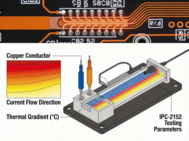
Running a trace at its theoretical limit will make it hot—sometimes too hot for surrounding components or human contact. Design for acceptable temperature rise, typically 10-20°C above ambient for reliable long-term operation.
High current through resistance equals voltage drop. In battery-powered applications, this can mean premature shutdown. In power distribution, it can cause uneven load sharing. Calculate IR drop for all significant current paths.
The bus bar or trace is only as good as its connections. Cold solder joints, loose bolts, and corroded contacts are failure points waiting to happen. Pay as much attention to connection design as to conductor sizing.
So who wins in the bus bar vs PCB trace showdown? The honest answer: it depends entirely on your application requirements.
For most low to moderate current applications, PCB traces remain the elegant, cost-effective solution. Modern Pcb Design tools and heavy copper options extend their practical range significantly.
For true high current applications—anything above 50-100 amps or where trace widths become impractical—bus bars become not just beneficial but necessary. The engineering challenge shifts from "can we route this on the PCB?" to "how do we integrate bus bars optimally into our system?"
The best approach often combines both: PCB traces for signal integrity and local distribution, bus bars for main power rails. Understand the trade-offs, design appropriately, and always verify with thermal testing.
Power Electronics Design is equal parts art and science. May your voltage drop be minimal and your temperature rise be controlled.
There's no single answer—it depends on trace width, Copper Thickness, layers, temperature rise allowed, and board environment. A rough guideline: 1 oz copper external trace can carry about 1 amp per mm of width for a 10°C rise. So a 10mm wide trace handles roughly 10 amps. Heavy copper (2-4 oz) proportionally increases capacity.
Consider bus bars when trace width requirements become impractical (exceeding 20-30mm), when you need to move more than 50-100 amps, when space constraints prevent adequate trace geometry, or when thermal management becomes problematic. Each application differs, but these thresholds typically indicate bus bar territory.
Bus bars can offer better reliability in demanding environments due to superior thermal dissipation, mechanical robustness, and vibration resistance. However, they introduce additional connections that could fail. PCB-integrated solutions eliminate this risk but may have manufacturing limitations. Reliability depends more on proper design and quality than on the choice between trace or bus bar.
Bus bar capacity depends on cross-sectional area, material, cooling method, and acceptable temperature rise. General formula: Current ≈ k × Area^0.7 × (Temperature Rise)^0.5, where k depends on material and cooling. For copper in free air, roughly 200-250 amps per square inch of cross-section with 30°C rise. Use manufacturer data or thermal simulation for critical applications.
Absolutely—and this is common in practice. Use PCB traces for signal distribution, low-current power rails, and connections within a board. Use bus bars for main power distribution between boards, high-current rails, or connections to external components. This hybrid approach often provides the best balance of cost, performance, and manufacturability.
Exceeding Trace Current Capacity leads to excessive heating, which can cause: solder joint failures, delamination of PCB layers, component damage from heat, copper electromigration, and eventually trace burnout or fire. Always design with adequate margin and include protection mechanisms for fault conditions.
IPC-2152 Current Carrying Capacity: The Definitive PCB Trace Calculator GuideMay/21/2026
Best Material for High Current PCB Design: How to Choose the Right SubstrateJune/05/2026
High Current PCB Design GuidelinesMay/21/2026
High Current PCB Connector Selection Guide: Choosing the Right Power Connectors for Your Electronics ProjectsJune/12/2026
High Current PCB Trace Width Calculator: The Ultimate Engineering GuideMay/20/2026
IPC-2152 Current Carrying Capacity Calculation GuideJune/03/2026
Best Material for High Current PCB DesignMay/21/2026
5 Critical Thermal Management Problems in High Power PCBsMay/21/2026