

Grounding strategy represents one of the most critical decisions in High Current Pcb Design. Whether you are building a motor drive, power supply, or battery management system, the way you handle ground connections directly impacts performance, efficiency, and electromagnetic compatibility. Among the available approaches, star ground and ground plane topologies dominate practical implementations, each offering distinct advantages for specific applications.
Understanding when to use each approach requires examining the underlying physics of current flow, impedance characteristics, and noise coupling mechanisms. This knowledge enables engineers to make informed decisions that optimize board performance while minimizing potential reliability issues.
Ground in an electronic circuit serves multiple purposes. It provides a reference voltage, a return path for current, and a shield against electromagnetic interference. In High Current applications, the ground return path becomes particularly important because significant current flowing through trace impedance generates voltage drops that can cause measurement errors, noise injection, and unexpected behavior.
The impedance of a ground path depends on Trace Geometry, material properties, and frequency content of the current. DC resistance causes static voltage drops, while AC impedance from skin effect and Loop Inductance creates dynamic voltage variations that are often more problematic than static offsets. Managing both requires careful attention to trace width, Copper Weight, and routing topology.
Low current circuits often treat ground as an equipotential node with negligible impedance. This assumption breaks down when currents reach tens of amperes or more. A ground trace that drops 50 millivolts across its length might be insignificant in a microamp-level signal circuit but catastrophic in a 50-amp Motor Controller where that voltage directly affects the measurement accuracy of current sense resistors.
High Current also increases electromagnetic field strength around conductors. These fields couple energy into nearby signal traces through mutual inductance, creating noise on sensitive measurement channels. Proper ground design must account for both the DC voltage drop problem and the AC noise coupling issue simultaneously.
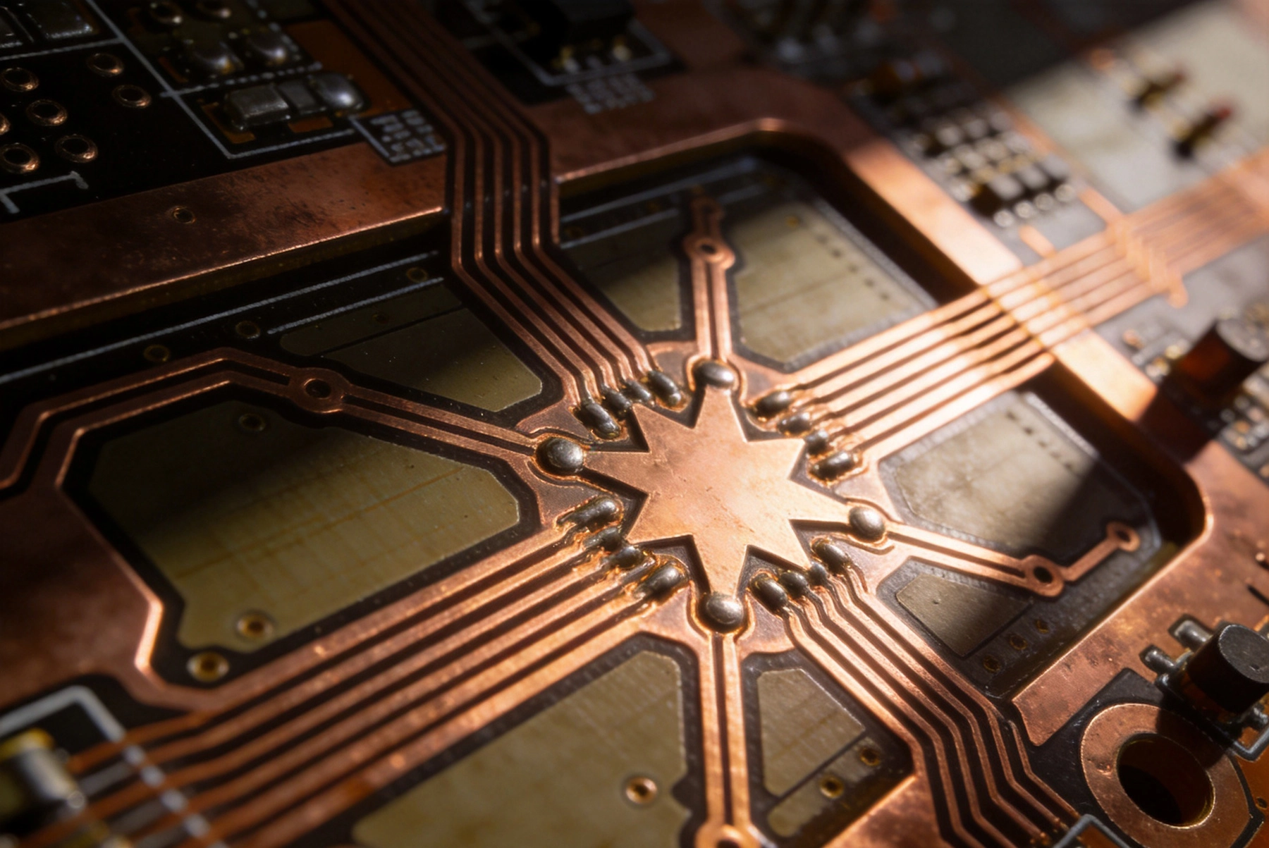
Star grounding connects all ground returns to a single central point, creating a radial topology reminiscent of a star shape. Each subsystem or circuit block returns to this central node rather than sharing ground paths with other circuits. This arrangement prevents one circuit's ground current from flowing through another circuit's ground return, eliminating a common source of noise and interference.
The star ground point typically connects to the system ground at a single location, often near the power entry point or main filter capacitor. From this central node, separate ground traces or planes branch to each functional block. The key principle is that no two circuits share a ground return path between them and the star point.
Star grounding excels in applications where circuit blocks have significantly different ground current magnitudes or noise characteristics. In a mixed-signal system, for example, sensitive analog circuits can share ground paths with noisy digital logic only through a carefully controlled star point, preventing digital switching noise from corrupting analog measurements.
The technique also simplifies Ground Loop analysis. With a single known ground point, tracing current paths becomes straightforward. Engineers can predict voltage drops at any node by calculating the current flowing through the impedance between that node and the star point. This predictability aids debugging and design verification.
Star grounding presents challenges when applied to high Current Distribution. The single point becomes a bottleneck where all ground current converges. If the trace or plane connecting to this point is undersized, significant voltage drops accumulate before current reaches peripheral circuits. Designers must size the trunk connection to the star point for the total system current, which can require very wide traces or Heavy Copper.
Additionally, the radial topology works against efficient current return in planar PCB constructions. Ground traces from the star point to peripheral circuits must travel long distances, increasing loop area and inductance. For very high current applications where efficiency matters, this topology can introduce more losses than it prevents.
Ground plane topology uses a continuous low-impedance copper region, typically on an inner layer or the board bottom, to distribute ground throughout the circuit. Current spreads across the plane according to its impedance distribution, taking multiple parallel paths rather than following a single designated route. This parallelism naturally minimizes total impedance and reduces voltage drops across the plane.
The ground plane works particularly well for high frequency Current Distribution because the skin effect forces current to spread evenly across the copper surface, reducing effective resistance. At lower frequencies, current distribution follows ohmic resistance, which also tends toward even spreading across large copper areas. Both mechanisms favor the plane topology for minimizing impedance.
Ground planes provide inherently low impedance return paths because they offer maximum cross-sectional area for current flow. A ground plane covering a significant portion of the board with one-ounce or two-ounce Copper Thickness presents milliohm or sub-milliohm impedance to current flow, keeping voltage drops negligible even at hundreds of amperes.
The plane also provides excellent thermal conductivity, spreading heat from high-current components across a large area. This thermal benefit becomes critical in Power Electronics where localized heating from components like MOSFETs or diodes can damage adjacent circuits. A well-designed ground plane acts as both electrical conductor and emergency heat spreader.
While ground planes offer superior impedance characteristics, they introduce new challenges related to current path predictability. Unlike star ground where engineers can calculate exact current paths, plane current distribution depends on the location of source and sink connections, producing complex patterns that vary with load conditions.
This unpredictability becomes problematic when sensitive circuits share ground planes with high current switching circuits. The changing current distribution under different load conditions creates voltage gradients across the plane that can appear as noise in measurement circuits. Careful Component Placement and strategic splits can mitigate these effects but require more design effort than star ground.
Ground planes consistently outperform star ground in impedance tests. The parallel current paths in a plane reduce effective resistance and inductance compared to single-trace star ground routes. For applications where minimizing voltage drop matters, such as high-precision current sensing, the plane topology provides clear advantages.
However, impedance is only part of the story. The voltage gradient across a ground plane, while typically small, exists throughout the plane surface. Two circuits connected to different points on the same plane experience slightly different ground potentials. In star ground, circuits connected to the same star point experience identical ground potential by definition, though at the cost of larger voltage drops to reach distant points.
Ground planes provide natural shielding against electromagnetic interference because the continuous copper region blocks field penetration from external sources. The plane also returns radiated emissions from internal switching circuits to their source, reducing overall EMI signature when properly implemented.
Star ground configurations can exhibit higher EMI because ground return traces act as antennas that radiate energy. The narrow geometry of individual ground traces provides no shielding and can couple noise between circuits through shared impedances. Careful routing and shielding become necessary when using star ground in noisy environments.
Star ground designs often require fewer layers because ground connections route as normal traces. This simplicity reduces Manufacturing Cost and improves yield. Ground planes typically require multilayer boards to accommodate signal layers and the plane layer simultaneously, increasing cost and complexity.
However, some ground plane implementations can actually reduce overall board area. The efficient current distribution in a plane often permits smaller conductors than equivalent star ground routes, potentially offsetting the cost of additional layers with reduced board size. Total cost analysis should consider both material and manufacturing factors.
Many high current designs combine star and plane concepts to leverage the strengths of each approach. A typical hybrid strategy uses a solid ground plane for the high current power section while implementing star ground topology for sensitive measurement and control circuits. The two domains connect at a single strategic point that serves as the system star ground.
This separation isolates high current switching noise from measurement circuits while maintaining low-impedance return paths for power currents. The technique requires careful planning of the connection point and often uses physical barriers or cutouts in the plane to reinforce the separation between domains.
Splitting ground planes creates distinct regions for analog and digital or power and signal circuits. Each region maintains its own ground reference while connecting to a common star point through a controlled impedance link. Ferrite beads, inductors, or narrow traces between regions provide high-impedance AC connections while maintaining DC continuity for bias purposes.
The split plane approach works well in mixed-signal applications where analog precision matters alongside digital processing. Power Electronics with sensitive current sense amplifiers similarly benefit from isolated ground regions that prevent switching transients from corrupting measurements. The key is ensuring that the single connection point between regions handles all inter-domain ground current without introducing problematic voltage drops.
Regardless of topology chosen, ground conductors must handle expected current without excessive voltage drop. Use IPC current capacity charts to determine minimum trace widths, then add margin for unexpected loads and temperature effects. For very high currents, bus bars, parallel traces, or Heavy Copper planes become necessary.
When using ground planes, verify Copper Weight and thermal relief specifications with your manufacturer. Standard PCB processes may not deliver expected current capacity if thermal reliefs or via registration reduce effective copper cross-section. Direct immersion plating or heavy copper options provide extra margin for demanding applications.
Position ground connections to minimize loop area and reduce exposed conductor length. For plane-based designs, place source and return connections close together to keep high current loops small. For star ground designs, route longer traces to lower-current circuits first, reserving the shortest paths for highest-current loads.
Current sense resistor placement deserves special attention. These components should connect directly to the ground reference point with minimal trace length, ensuring that voltage drop across sense traces does not affect measurement accuracy. Kelvin connections that separate current flow from measurement voltage provide the cleanest sense signal regardless of ground topology.
High current ground paths generate heat proportional to current squared and impedance. This heating affects both reliability and performance. Ground planes naturally spread thermal load, while narrow traces concentrate heat at high-resistance points like vias or connections.
Consider thermal simulation for high current designs, especially where ground connections pass through thermal bottlenecks like vias or narrow neck-down regions. Adding thermal relief strategies, additional vias, or wider copper around hotspots maintains temperature within acceptable limits and prevents premature failure from thermal stress.
Many engineers treat ground as zero impedance without calculation. This assumption works for low-current circuits but creates serious problems in power applications. Always calculate expected voltage drop across ground paths under maximum load conditions, even if preliminary analysis suggests the result is small.
Measure actual voltage differences between ground points during prototype testing. Discrepancies between calculated and measured values often reveal impedance sources not considered in the original analysis. Documenting these findings improves future designs and validates simulation assumptions.
DC resistance calculations ignore frequency-dependent effects that matter for switching power supplies and motor control circuits. Switching transients contain high-frequency components that see higher impedance in narrow conductors due to skin effect. Wide traces, solid planes, and careful via placement reduce high-frequency impedance.
For designs with switching frequencies above 100 kHz, consider using transmission line techniques for ground connections. Controlled impedance ground returns adjacent to high-speed signal traces maintain signal integrity while providing low-impedance current paths. This technique requires more sophisticated design tools but yields superior performance.
Ground loops occur when multiple current paths create circulating currents in the ground system. While sometimes beneficial for shielding, ground loops in power circuits create unpredictable voltage drops and potential oscillation. Careful routing that prevents overlapping current return paths avoids these problems.
Star ground topology inherently prevents ground loops by ensuring single current paths. Plane-based designs require more attention to current flow paths to avoid unintentionally creating loop configurations. Following the principle that current returns along the path of least impedance, which usually means the shortest path, guides placement decisions.
Prototype testing should verify that ground design meets performance requirements under worst-case conditions. Measure voltage differences between ground points under full load, checking for unexpected drops or noise coupling. Thermal imaging during operation reveals hotspots caused by excessive Current Density or poor thermal relief.
EMI testing validates that ground design adequately contains radiated emissions and withstands external interference. Pre-compliance testing with spectrum analyzers and near-field probes identifies problems before formal certification testing. Early detection allows design iterations that address issues before production tooling commits the design.
High Current Pcb grounding requires careful consideration of topology trade-offs between star ground and ground plane approaches. Star ground offers simplicity and predictable ground potentials but can introduce higher impedance and larger loop areas. Ground planes provide superior electrical performance but require more complex design and potential separation between sensitive and noisy circuits.
Hybrid approaches that combine star and plane techniques often deliver the best results in demanding applications. Separating high current power grounds from sensitive measurement grounds while connecting at a single strategic point leverages the advantages of both topologies. This strategy requires upfront planning but prevents performance problems that prove expensive to fix after production launch.
The specific requirements of your application drive the optimal choice. Motor control circuits with sensitive current sensing benefit from plane-based grounds that minimize voltage drops. Mixed-signal systems with widely varying ground current magnitudes often work better with star ground isolation between domains. Understanding the underlying principles enables confident decisions that result in reliable, high-performance products.
Star ground works best when circuit blocks have very different current levels or noise characteristics that you need to isolate. It also suits applications where predictable ground potentials matter more than absolute impedance, or where multilayer boards are impractical. Consider star ground for mixed-signal designs with sensitive analog circuits.
Use Ipc-2221 current capacity tables as a starting point, then apply safety margins. For example, a 10-ampere current might require approximately 100 mils (2.5mm) of 1-ounce Copper Trace Width for acceptable temperature rise. Higher currents or tighter temperature budgets require wider traces or heavier copper weights.
Yes, hybrid approaches are common and often optimal. Use solid ground planes for high current distribution while implementing star ground topology for sensitive measurement circuits. Connect both to a single strategic point that serves as the overall system ground reference.
Slots interrupt current flow and force current around obstacles, increasing path length and impedance. They also reduce thermal conductivity in affected areas. Minimize slots in high current regions, and ensure that any required slots do not create bottlenecks that force current through narrow paths.
Connect current sense resistors with short, wide traces directly to the ground reference point. Use four-wire Kelvin connections to separate current flow from measurement voltage. Route the sense connection to avoid sharing any trace length with high current paths to prevent measurement error from ground voltage drops.
High Current PCB Routing: 45-Degree Angles vs. Curved Traces in PracticeJuly/12/2026
High Current PCB Current Crowding: Sharp Corners vs. Teardrop TransitionsSeptember/03/2026
High Current PCB Solder Wicking: Tented Vias vs. Untented ViasSeptember/01/2026
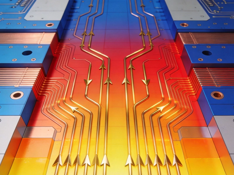
Overcoming Voltage Drop in High Current PCB Power Planes: A Case StudyJuly/13/2026

High Current PCB Design for Drone ESCs: Minimizing Loop InductanceAugust/03/2026
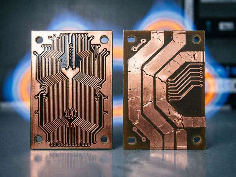
High Current PCB vs. Standard PCB: A Real-World Thermal Stress TestJuly/09/2026
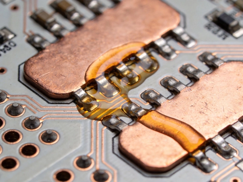
High Current PCB Solder Joints: Wave Soldering vs. Selective SolderingJuly/15/2026
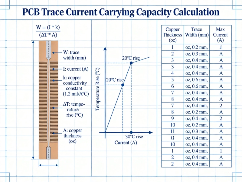
IPC-2152 Current Carrying Capacity: The Definitive PCB Trace Calculator GuideMay/21/2026