

Power Electronics place unique demands on printed circuit board design. When currents exceed a few amperes, Thermal Management becomes as critical as electrical performance. Thermal relief pads—the connections between component pads and copper planes—serve double duty: they must conduct heat effectively during soldering while maintaining low electrical resistance for power delivery. Understanding when to use full connections versus modified spoke patterns determines whether your high-current assemblies perform reliably or fail prematurely.

Thermal relief sounds like something you add to reduce heat, but the reality involves solderability rather than thermal isolation. When you solder a component to a large copper plane, the plane acts as a massive heat sink. Without relief features, solder refuses to melt properly because the copper plane draws away heat faster than your soldering iron can supply it.
The classic thermal relief pattern—four spoke-like connections between the component pad and surrounding plane—creates controlled Thermal Resistance. These narrow copper bridges limit heat flow into the plane while still providing adequate electrical connection. The technique works beautifully for standard components, but high-current applications complicate the picture significantly.
Power components like MOSFETs, regulators, and connectors often carry currents of 10A, 20A, or more. Current flowing through narrow thermal relief spokes creates resistive heating. Four thin connections may look fine on paper but generate enough heat to fail in the field or become impossible to solder without specialized equipment.
The fundamental tension emerges clearly: thermal relief spokes that facilitate soldering become current-limiting bottlenecks once assembled. Your design must balance manufacturability against electrical performance.
Full connect Thermal Design eliminates the traditional spoke pattern entirely. The component pad connects directly to the surrounding plane with solid copper. This approach delivers the lowest possible resistance and handles the highest current densities without heating concerns.
Electrical performance benefits immediately. Current flows through a broad copper bridge rather than narrow spokes, dramatically reducing resistive losses. Temperature rise from self-heating drops proportionally. For 20A+ applications, this difference can mean the difference between acceptable operating temperatures and thermal runaway conditions.
Mechanical reliability improves as well. Solid connections withstand vibration and Thermal Cycling better than delicate spoke patterns. Joints crack less frequently when the current path shares stress loads across broader copper rather than concentrating forces in narrow bridges.
Modern soldering equipment handles direct thermal connections effectively. Hot plate reflow, vapor phase soldering, and pre-heated IR stations all provide sufficient thermal energy to melt solder despite plane heat sinking. Manual soldering becomes challenging but not impossible with appropriate tools.
Full connect suits applications where manufacturing processes accommodate the thermal mass. If your assembly uses reflow processing, direct thermal connections rarely cause problems. The technique works particularly well for automated production where consistent process control ensures reliable solder joints regardless of thermal conditions.
Between full connect and classic four-spoke patterns lies a spectrum of modified configurations. These hybrid approaches attempt to optimize both thermal and electrical performance by adjusting spoke count, width, and geometry.
The simplest modification involves widening the standard spokes. Rather than 0.3mm traces connecting pad to plane, you might use 0.8mm or 1.0mm connections. Wider spokes handle more current while still providing some thermal relief for soldering.
This approach works well when moderate current levels—say 5-10A—require better conductivity than standard spokes provide but full connect seems excessive. The wider connections reduce resistance proportionally while maintaining manufacturing compatibility with conventional soldering approaches.
Adding more connection points distributes current across additional parallel paths. Six or eight spokes of equivalent width to a four-spoke pattern provide 1.5x or 2x the current handling capacity while preserving thermal relief characteristics.
The limitation emerges in pad geometry. Component pads have finite perimeter, and placing more connections requires smaller individual widths or creative pad shaping. Nonetheless, this technique provides meaningful improvement for applications in the 10-15A range.
Rotating spoke orientation or using asymmetric patterns addresses specific current flow requirements. For connectors and large pads, you might concentrate connections on the side where current enters and exits rather than distributing them evenly around the pad perimeter.
This approach requires careful analysis of current paths through the pad. Simulation tools help identify optimal spoke placement when designs approach thermal limits.
Modern Pcb Design increasingly relies on simulation to optimize thermal relief decisions rather than following rules-of-thumb blindly.
Current flowing through copper generates heat according to power dissipation formulas. The temperature rise depends on current magnitude, trace width or connection geometry, Copper Weight, and surrounding thermal conditions. Software tools fromcadence, Altium, and Thermal Analysis packages calculate temperature rise based on these parameters.
For thermal relief analysis, you model the spoke connections as narrow traces carrying specified current. The simulation reveals whether your chosen geometry maintains acceptable temperature rise or requires modification.
Advanced simulation approaches solve coupled thermal and electrical equations simultaneously. These tools account for how heating affects resistance (copper resistance increases with temperature), creating more accurate predictions than simple calculations.
Results guide geometry decisions by showing exactly where hotspots form and how design changes affect overall thermal performance. This level of analysis becomes worthwhile for demanding applications where over-design adds unnecessary cost.
While simulation provides detailed guidance, practical design often benefits from established heuristics refined through production experience.
Standard four-spoke thermal relief typically handles currents up to 3-5A reliably, depending on pad size and Copper Weight. Wider spokes (0.5-0.8mm) extend this range to perhaps 8-12A for six-connection configurations. Full connect designs handle virtually any current your copper weight can accommodate.
These ranges assume standard 1oz copper. Heavy Copper boards (2oz, 3oz, or more) extend current handling proportionally. The relationship isn't linear—doubling copper weight more than doubles current capacity because Thermal Resistance also improves.
High-current designs often incorporate vias directly in component pads to spread current into multiple board layers. This technique effectively increases copper cross-section but creates manufacturing challenges including Solder Wicking into vias.
Via filling and capping processes address Solder Wicking, but they add cost. Alternatively, dog-bone layouts route traces from pad to nearby vias positioned outside the solder zone. This approach increases routing complexity but maintains standard assembly processes.
Design decisions mean nothing if your manufacturing processes can't produce reliable assemblies. Matching thermal relief strategy to your assembly approach ensures designs translate into working products.
Reflow processes heat entire boards uniformly in controlled ovens, eliminating concerns about individual pad thermal mass. Full connect thermal designs work reliably in reflow environments because the board temperature equilibrates rather than depending on localized heat sources.
Vapor phase reflow proves particularly effective for high-thermal-mass designs because the phase-change medium transfers heat extremely efficiently. Even challenging full connect layouts solder consistently in vapor phase systems.
Prototyping and repair often require hand soldering where thermal relief matters critically. Here, modified spoke configurations or controlled thermal connections provide practical benefits. Designs intended for hand assembly should moderate thermal mass unless rework stations with pre-heating capabilities are available.
Selective Soldering machines offer middle-ground capabilities—they heat specific areas while protecting surrounding components. Understanding your assembly and rework capabilities should inform thermal relief choices.
Thermal relief decisions require clear documentation to ensure manufacturing partners understand your intent.
Clearly specifying thermal relief requirements in design documentation prevents manufacturing surprises. Note current-carrying requirements that drive your choices, and indicate whether full connect is intentional or requires special handling.
Gerber outputs don't communicate thermal relief strategy directly. Manufacturing notes, design intent documentation, or explicit callouts on assembly drawings convey requirements that wouldn't otherwise appear in fabrication data.
Experienced contract manufacturers recognize thermal relief trade-offs and can suggest improvements based on their process capabilities. Early engagement allows them to flag potential issues and propose modifications that enhance manufacturability without compromising electrical performance.
These conversations prove most valuable for new designs approaching current limits. Manufacturers who work with Power Electronics regularly have accumulated practical knowledge about what works reliably in their specific equipment.
Thermal relief design for high-current PCBs demands balancing competing requirements—manufacturability during assembly and reliable current delivery during operation. Full connect approaches maximize electrical performance but require appropriate manufacturing processes. Modified spoke configurations provide practical middle-ground options that accommodate both soldering and current handling needs.
No universal solution fits every application. Your specific current requirements, copper weights, assembly processes, and reliability expectations should guide thermal relief choices. Start with simulation to understand thermal implications, then refine designs based on manufacturing feedback.
The investment in thoughtful thermal relief design pays dividends in product reliability and manufacturing efficiency. Designs that work reliably in production outperform theoretically optimized layouts that cause assembly problems or field failures.
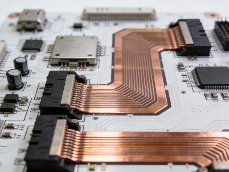
High Current PCB Design for Aerospace Power DistributionSeptember/08/2026
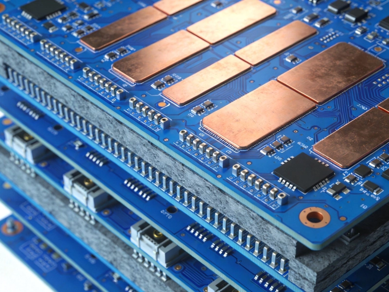
High Current PCB Design for Telecommunications Base StationsSeptember/18/2026
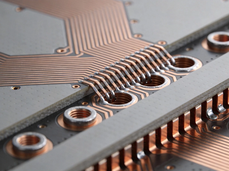
High Current PCB Thermal Vias: Array Spacing and Heat Transfer EfficiencySeptember/15/2026
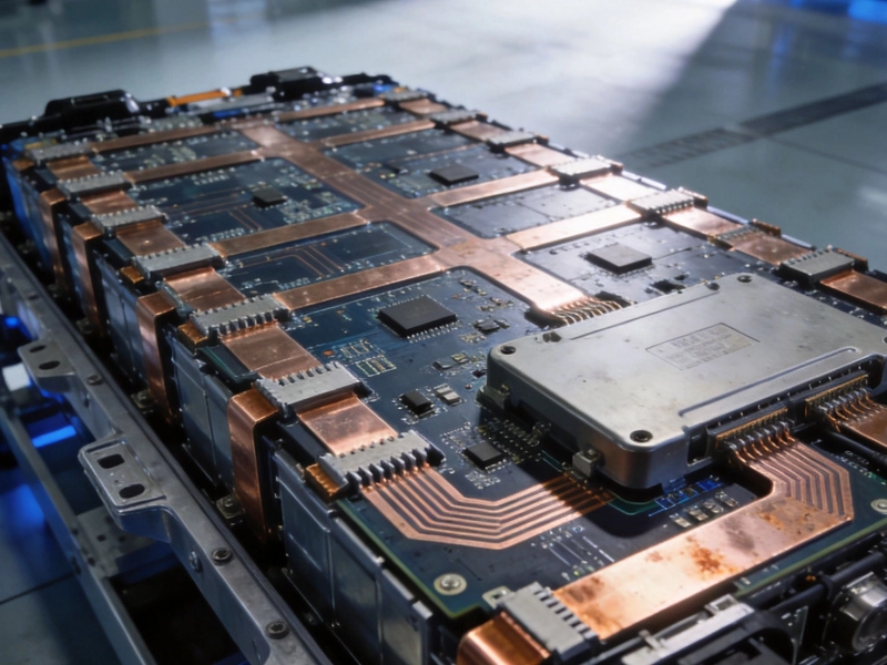
Designing a 100A High Current PCB for EV Battery Management SystemsJuly/09/2026
Why Your High-Power PCBs Overheat (And the 5 Methods That Actually Fix It)May/20/2026

High Current PCB Design for Medical Imaging EquipmentSeptember/10/2026
High Current PCB Design for Uninterruptible Power Supplies (UPS)September/02/2026
High Current PCB Design for Audio Amplifiers: Avoiding Ground LoopsSeptember/14/2026