

High Current PCB testing presents unique challenges that demand specialized measurement techniques. As electronics push toward higher power densities and increased current carrying requirements, accurate assessment of Pcb Current Capacity, voltage drop, and thermal performance becomes critical for product reliability and safety. Two dominant methods have emerged for evaluating High Current PCB performance: thermal imaging and 4-wire Kelvin measurement. Each approach offers distinct advantages, serving different testing scenarios and providing complementary insights into PCB behavior under High Current conditions.
Understanding when to apply thermal imaging versus 4-wire Kelvin measurement—or when to combine both approaches—can significantly improve your testing accuracy, reduce development time, and prevent costly field failures. This comprehensive analysis explores the technical foundations, practical applications, and decision criteria for both methods, helping you develop robust High Current Pcb testing strategies that match your specific requirements.
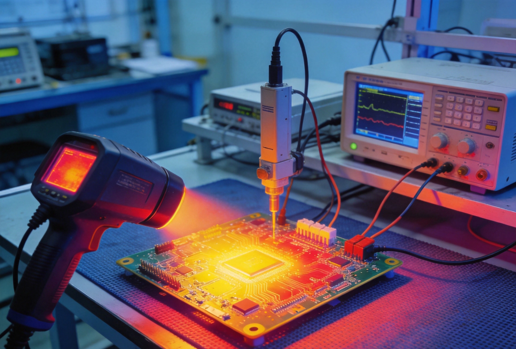
High Current Pcb testing differs fundamentally from low-voltage, low-current evaluation in several critical aspects. When PCBs carry currents exceeding 5-10 amps, several physical phenomena become significant:
High currents flowing through Pcb Traces, vias, and planes generate substantial resistive heating (I²R losses). This heating can cause temperature increases that affect Solder Joint Reliability, component lifespan, and overall system performance. The relationship between current, resistance, and temperature rise is non-linear and depends heavily on Pcb Layout, Copper Thickness, Thermal Management strategies, and environmental conditions. Accurate thermal assessment requires understanding heat generation, dissipation paths, and steady-state versus transient thermal behavior.
At high currents, even trace resistances as low as a few milliohms can cause significant voltage drops that impact circuit performance. Power Distribution networks must maintain adequate voltage margins throughout the PCB while delivering required current to all loads. Measuring these small voltage drops accurately presents challenges because measurement leads and connections introduce their own resistances that can distort readings. This is particularly critical for Power Integrity analysis, where millivolt-level accuracy matters for determining proper operation.
Current doesn't distribute uniformly across PCB conductors, especially at high frequencies where skin effect becomes significant. Even at DC and low frequencies, geometric factors, via placement, and Trace Geometry can cause Current Crowding in specific areas, creating localized hotspots that may exceed safe operating temperatures. Understanding Current Distribution patterns helps identify potential failure points and optimize Trace Geometry for better Current Carrying Capacity and thermal performance.
High Current PCB failures can have serious consequences, ranging from reduced product lifespan to catastrophic thermal events leading to fire or safety hazards. Testing must therefore not only verify that PCBs meet specifications under normal operating conditions but also identify marginal designs that might fail under worst-case scenarios like elevated ambient temperatures, reduced cooling, or transient current spikes. Comprehensive testing helps ensure long-term reliability and compliance with safety standards across the product's intended operating envelope.
Thermal imaging, also known as infrared (IR) thermography, provides non-contact temperature measurement across an entire PCB surface simultaneously. Modern thermal imaging cameras detect infrared radiation emitted by objects and convert it into temperature readings, creating visual thermal maps that reveal hotspots, thermal gradients, and overall thermal performance under operating conditions.
Thermal imaging cameras capture infrared radiation in the wavelength range of approximately 8-14 micrometers, which corresponds to the peak emission of objects at typical PCB operating temperatures (25-150°C). The camera's detector array measures infrared intensity at each pixel, and sophisticated algorithms convert these measurements into temperature values based on the object's emissivity, ambient temperature, and atmospheric conditions. Advanced cameras provide temperature accuracy of ±2°C or better, with thermal sensitivity down to 0.05°C for detecting subtle temperature variations.
The resulting thermal image displays temperature information as color gradients, with warmer areas typically shown in red, orange, or yellow, and cooler areas in blue or green. This visual representation immediately highlights thermal problems like overloaded traces, undersized vias, poor thermal connections, or inadequate cooling. Many cameras also provide spot temperature measurement, area analysis, and isotherm tools for quantitative Thermal Analysis.
Thermal imaging offers several compelling advantages for high current PCB testing:
Unlike point measurement techniques that examine only specific locations, thermal imaging captures temperature data across the entire PCB surface simultaneously. This comprehensive view reveals thermal interactions between components, traces, and planes that might be missed with selective measurements. You can identify unexpected hotspots, thermal coupling effects, and cooling inefficiencies that point measurements might never discover.
Thermal imaging requires no physical contact with the PCB, eliminating measurement loading effects that could alter the thermal behavior you're trying to measure. This is particularly important for high current applications where attaching thermocouples or other sensors might affect Heat Dissipation paths or introduce additional thermal mass that changes thermal time constants. Non-contact measurement also allows testing of operating PCBs without disrupting normal function or introducing safety hazards associated with attaching probes to high voltage/high current circuits.
Modern thermal cameras can capture thermal images at frame rates exceeding 60 Hz, enabling real-time monitoring of thermal transients and dynamic thermal behavior. This capability proves invaluable for studying thermal behavior during power-up sequences, load changes, or fault conditions. Time-lapse thermal imaging can track temperature evolution over extended periods, helping verify Thermal Management design and identify long-term thermal stability issues.
The intuitive visual nature of thermal images makes thermal problems immediately obvious to engineers, technicians, and even non-technical stakeholders. Hotspots jump out clearly from cooler areas, accelerating problem diagnosis and facilitating communication about thermal issues across teams. This visual clarity also supports documentation for design reviews, failure analysis reports, and regulatory submissions.
Despite its strengths, thermal imaging has important limitations for high current PCB testing:
Thermal imaging measures only surface temperatures, providing no direct information about internal temperatures of buried traces, vias, or internal planes. For multilayer PCBs where critical current paths reside on inner layers, thermal imaging alone cannot provide complete thermal assessment. You must infer internal thermal behavior from surface patterns or combine thermal imaging with other measurement techniques.
Accurate temperature measurement requires knowledge of surface emissivity—the efficiency with which a surface emits infrared radiation. Different PCB materials have different emissivities (typically 0.85-0.95 for solder mask, 0.05-0.15 for exposed copper), and surface conditions like oxidation, contamination, or coating can significantly affect emissivity. Inaccurate emissivity values can introduce temperature errors of 10-20°C or more, requiring careful calibration and correction.
Thermal cameras balance spatial resolution against field of view. Wide field of view cameras capture the entire PCB but may lack the resolution to examine fine details like individual traces or small components. High-resolution cameras provide detailed thermal data but may require multiple images to cover large boards, complicating analysis and potentially missing thermal interactions between different board areas.
Shiny surfaces like exposed copper or metal components can reflect infrared radiation from surrounding objects, creating false thermal readings. Similarly, some PCB materials may be partially transparent to infrared radiation, allowing radiation from underlying layers to affect surface temperature measurements. These optical effects require careful consideration and may necessitate surface treatments or alternative measurement approaches.
4-wire Kelvin measurement, also known as 4-wire sensing or Kelvin Connection, provides highly accurate resistance and voltage drop measurements by eliminating the influence of test lead resistance and contact resistance. This technique proves particularly valuable for high current PCB testing where measuring small voltage drops across low-resistance paths requires milliohm or micro-ohm accuracy.
The 4-wire Kelvin method uses separate pairs of leads for current sourcing and voltage sensing. One pair of leads (force leads) carries the test current through the device under test, while a second pair (sense leads) measures the voltage drop across the device at precisely the points where current enters and exits. Because sense leads carry negligible current (typically microamps to milliamps), the voltage drop across the sense leads themselves is minimal, and contact resistance between sense probes and the device under test has negligible effect on the measured voltage.
The fundamental principle is that the voltage measured by the sense leads equals the device's true terminal voltage, unaffected by the resistance of force leads or their contact points. By measuring both the current through the device (via the force leads) and the voltage across it (via the sense leads), you can calculate resistance with high accuracy using Ohm's Law (R = V/I). This approach eliminates errors that would otherwise be introduced by lead resistance, contact resistance, and connection quality.
4-wire Kelvin measurement offers several critical advantages for high current PCB testing:
4-wire Kelvin measurement can achieve resistance measurement accuracy of 0.1% or better, with resolution down to micro-ohms. This level of accuracy proves essential for evaluating voltage drop in Power Distribution networks, trace resistance verification, and contact resistance assessment. For high current applications where millivolt-level voltage drops significantly impact performance, this accuracy enables precise design verification and optimization.
By separating current-carrying and voltage-sensing functions, 4-wire measurement completely eliminates the influence of test lead resistance on measurements. This is particularly important for high current testing where long test leads or small-gauge wire might introduce significant resistance that would distort 2-wire measurements. Force leads can be thin and inexpensive since their resistance doesn't affect measurement accuracy, while sense leads carry minimal current and can be very fine without introducing errors.
Contact resistance between measurement probes and the device under test can vary significantly depending on probe type, pressure, surface condition, and oxidation. In 2-wire measurements, this variable contact resistance introduces measurement uncertainty. 4-wire measurements are virtually unaffected by sense lead contact resistance because sense current is so small that even milliohm-level contact resistances cause negligible voltage drops. This makes 4-wire measurements highly repeatable even with imperfect probe contacts.
Unlike thermal imaging, which measures thermal effects as indirect indicators of electrical behavior, 4-wire Kelvin measurement provides direct electrical performance data. You measure the actual resistance and voltage drop that affect circuit operation, enabling precise correlation with electrical specifications and performance requirements. This direct measurement approach supports quantitative design verification and tolerance analysis that thermal methods cannot provide.
Despite its accuracy advantages, 4-wire Kelvin measurement has important limitations:
4-wire measurement provides data only at specific measurement points, giving no information about what happens between those points. To create a complete picture of PCB electrical performance, you must take multiple measurements at various locations, which can be time-consuming and may miss localized problems between measurement points. This contrasts with thermal imaging, which provides continuous spatial coverage.
4-wire measurement requires physical access to test points where you can make four separate probe connections. For populated boards, this may mean measuring at test pads, component leads, or carefully probing at specific locations. Making reliable 4-wire connections to fine-pitch components, BGA devices, or inner-layer traces can be challenging or impossible without dedicated test fixtures or specially designed test points.
Performing 4-wire measurements across multiple test points on a PCB is inherently slower than capturing a single thermal image. Each measurement requires careful probe placement, connection verification, and data recording. For comprehensive characterization of large boards or complex power distribution networks, the time investment can be significant, especially if measurements must be repeated under different operating conditions.
To perform meaningful 4-wire resistance measurements on high current paths, you must flow substantial test currents through the device under test—often several amps or more to achieve adequate signal-to-noise ratio in small voltage measurements. This requires capable current sources, appropriate safety precautions, and careful management to avoid damaging the PCB or components during testing. Managing high test currents adds complexity compared to thermal imaging's passive observation approach.
Understanding the strengths and limitations of each technique helps you select the most appropriate approach for specific testing scenarios:
Successful implementation of either testing method requires attention to practical considerations that affect measurement quality and usability:
For accurate and useful thermal imaging results:
For reliable 4-wire Kelvin measurements:
Investment requirements differ significantly between the two approaches:
Entry-level thermal cameras suitable for basic PCB thermal imaging cost $2,000-$5,000 and provide temperature accuracy of ±2-5°C with thermal resolution of 0.1°C. Professional-grade cameras offering ±1-2°C accuracy, 0.05°C thermal sensitivity, and advanced analysis features typically cost $10,000-$30,000. High-end research cameras with sub-millikelvin sensitivity and specialized capabilities can exceed $100,000. Additional costs may include calibration services, specialized lenses, software licenses, and mounting fixtures.
Basic 4-wire measurement capabilities can be implemented with a precision current source ($1,000-$3,000) and a high-resolution digital multimeter ($500-$2,000) that supports 4-wire resistance measurement modes. Dedicated micro-ohmmeters with integrated 4-wire capability range from $3,000-$15,000 depending on accuracy, resolution, and current range. Kelvin probe sets cost $200-$1,000 depending on quality and features. For automated testing, switch matrices and fixture design add additional costs but enable high-throughput production testing.
Thermal imaging typically involves higher upfront equipment costs but enables faster, more comprehensive testing that can reduce total test time and labor costs. 4-wire Kelvin measurement requires lower initial investment but may involve more time-consuming manual testing unless automated. Many organizations find that investing in both capabilities provides the most comprehensive testing approach, with each technique complementing the other's strengths.
Effective high current PCB testing requires integration throughout the product development lifecycle:
Use simulation tools to predict thermal behavior and electrical performance, then validate predictions with early prototype testing. Combine thermal imaging with 4-wire measurements to confirm that trace resistances, via capacities, and thermal management approaches meet design targets. Use these early measurements to refine design rules and simulation models before finalizing the design.
Conduct comprehensive thermal and electrical characterization across multiple operating conditions, including worst-case scenarios like maximum current, elevated ambient temperature, and reduced cooling. Document thermal behavior at different power levels and load configurations. Use 4-wire measurements to verify that voltage drops remain within specifications across all operating conditions.
Establish quality control procedures based on validated test methods. For thermal validation, use thermal imaging to verify that production units perform similarly to qualified prototypes. For electrical verification, implement 4-wire measurement procedures at critical test points to ensure consistent electrical performance. Develop acceptance criteria based on characterization data from qualified units.
When field failures occur, use both thermal imaging and 4-wire measurements to investigate root causes. Thermal imaging can reveal abnormal thermal patterns that might indicate design margins, manufacturing defects, or application misuse. 4-wire measurements can identify resistance changes that might indicate connection problems, material degradation, or assembly issues.
High current PCB testing continues evolving with advancing technology:
Continued improvements in detector technology are delivering thermal cameras with higher spatial resolution, better temperature accuracy, and faster frame rates. Microbolometer arrays with 640×512 or higher pixel counts provide detailed thermal mapping of fine-pitch components and narrow traces. Uncooled detectors with noise-equivalent temperature difference (NETD) below 20mK enable detection of subtle thermal variations.
Artificial intelligence and machine learning algorithms are being integrated with thermal imaging to automatically identify anomalies, classify thermal patterns, and predict potential failure points. These automated analysis tools reduce interpretation time and improve consistency across different operators and testing sessions.
Combined test platforms that integrate thermal imaging, 4-wire electrical measurement, and automated test sequencing are emerging for comprehensive high current PCB validation. These systems can perform correlated thermal and electrical measurements under controlled conditions, providing richer datasets for design validation and quality assurance.
Emerging technologies like magnetic field imaging and current-sensing camera systems promise to provide non-contact Current Distribution mapping that complements thermal imaging's non-contact temperature measurement. These approaches could enable fully non-contact characterization of both thermal and electrical performance in the future.
Thermal imaging and 4-wire Kelvin measurement represent complementary approaches to high current PCB testing, each offering unique advantages for different testing scenarios. Thermal imaging provides comprehensive, non-contact thermal assessment that quickly reveals thermal problems across entire board surfaces. 4-wire Kelvin measurement delivers exceptional electrical accuracy for resistance and voltage drop characterization, enabling quantitative verification of electrical performance specifications.
The most effective high current PCB testing strategies leverage both methods, using thermal imaging for rapid thermal screening and problem identification, then applying 4-wire Kelvin measurement for detailed electrical characterization and quantitative verification. Understanding when to apply each technique—and how to interpret their results together—enables more comprehensive testing, faster problem resolution, and more reliable high current PCB designs.
As electronics continue pushing toward higher power densities and increased current requirements, the importance of accurate, comprehensive testing only grows. Investing in both thermal imaging and 4-wire measurement capabilities provides the tools needed to meet these challenges, supporting development of robust, reliable high current PCBs that perform as intended across their intended operating envelopes.
No, thermal imaging only measures surface temperatures. For multilayer PCBs with critical internal current paths, you must infer internal thermal behavior from surface patterns, use thermal simulation, or combine thermal imaging with other techniques like embedded temperature sensors or finite element analysis to estimate internal temperatures.
Choose a test current that provides adequate voltage signal for accurate measurement without causing excessive heating or risk of damage. A good starting point is 10-20% of the expected operating current, adjusted based on the measured voltage drop and observed thermal effects. For very low resistance measurements, you may need higher currents—always verify that the device under test can handle the chosen test current without damage.
With proper calibration and emissivity settings, modern thermal cameras can achieve temperature accuracy of ±1-2°C for PCB applications. However, this accuracy requires careful attention to emissivity values, environmental conditions, and camera settings. For the best accuracy, validate thermal camera measurements against contact thermocouple measurements at known reference points.
For high current PCB testing where you're measuring very low resistances (milliohms or less), 2-wire measurements typically introduce unacceptable errors due to lead resistance and contact resistance. 4-wire Kelvin measurement eliminates these errors and is strongly recommended for accurate high current PCB resistance and voltage drop measurements.
Start by defining your testing objectives. If you need to identify hotspots, verify thermal management, or visualize thermal behavior across the entire board, thermal imaging is the appropriate choice. If you need to measure very low resistances, verify voltage drop specifications, or characterize contact resistance with high accuracy, 4-wire Kelvin measurement is the better approach. For comprehensive characterization, use both techniques to capture both thermal and electrical performance data.
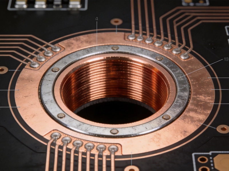
High Current PCB Annular Rings: Minimum Size vs. Reinforced SizeAugust/12/2026
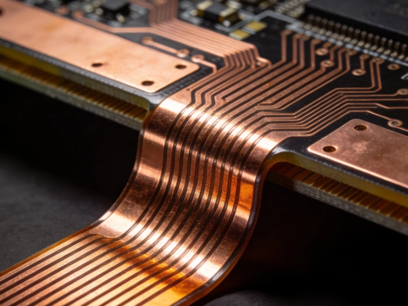
High Current PCB Flex-Rigid: Current Capacity in Bend AreasOctober/09/2026
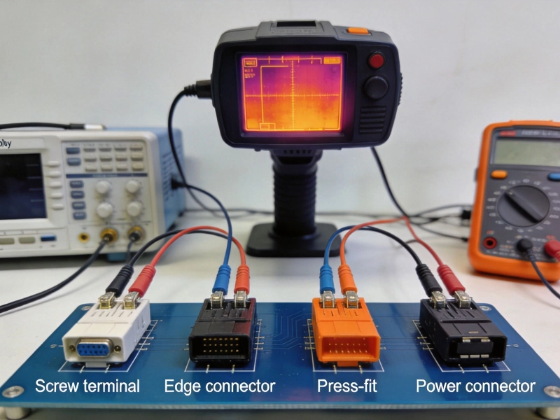
High Current PCB Connector Selection: Test Results and Real Performance DataMay/21/2026
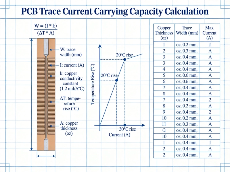
IPC-2152 Current Carrying Capacity: The Definitive PCB Trace Calculator GuideMay/21/2026
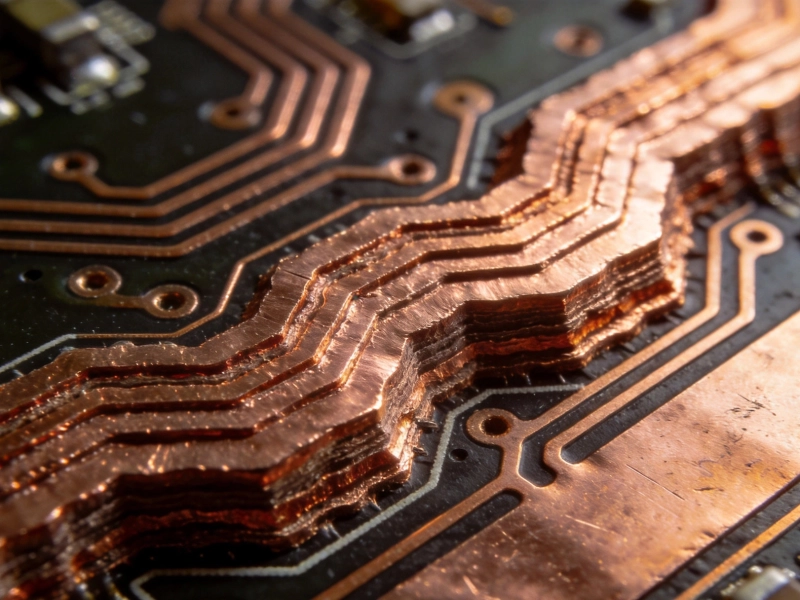
High Current PCB Bus Bars vs. Heavy Copper Traces: Cost and PerformanceJuly/25/2026
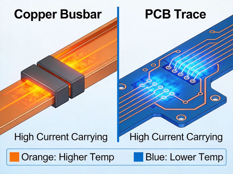
Bus Bar vs PCB Trace for High CurrentMay/21/2026
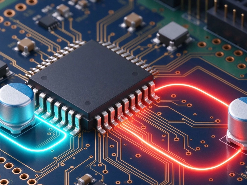
High Current PCB Decoupling Caps: Placement Distance vs. Loop AreaOctober/12/2026
High Current PCB Via Plating: 1mil vs. 2mil Thickness Reliability TestAugust/03/2026