

Every PCB designer who works with Power Electronics eventually confronts a fundamental tension: the need to move high currents through a multilayer board while keeping manufacturing costs within budget. Blind vias make this challenge more acute. They offer the routing flexibility that complex multilayer designs demand, but they also introduce manufacturing complexity that translates directly into higher per-board cost. Understanding how to balance Current Carrying Capacity against fabrication expense is a practical skill that separates effective power board designers from those who either over-engineer and overpay, or under-design and discover reliability problems in the field.
High-current applications in boards are increasingly common. Electric Vehicle controls, motor drives, power conversion systems, battery management circuits, and LED lighting all require Pcb Traces and vias that can handle amperes or even tens of amperes without excessive temperature rise. In a multilayer board, the current path frequently crosses between layers, which means vias must carry a substantial portion of the total current. Standard through-hole vias may not provide enough cross-sectional copper area, and the designer must decide whether to use multiple smaller vias, fewer large vias, or more sophisticated structures like blind vias with Heavy Copper plating.
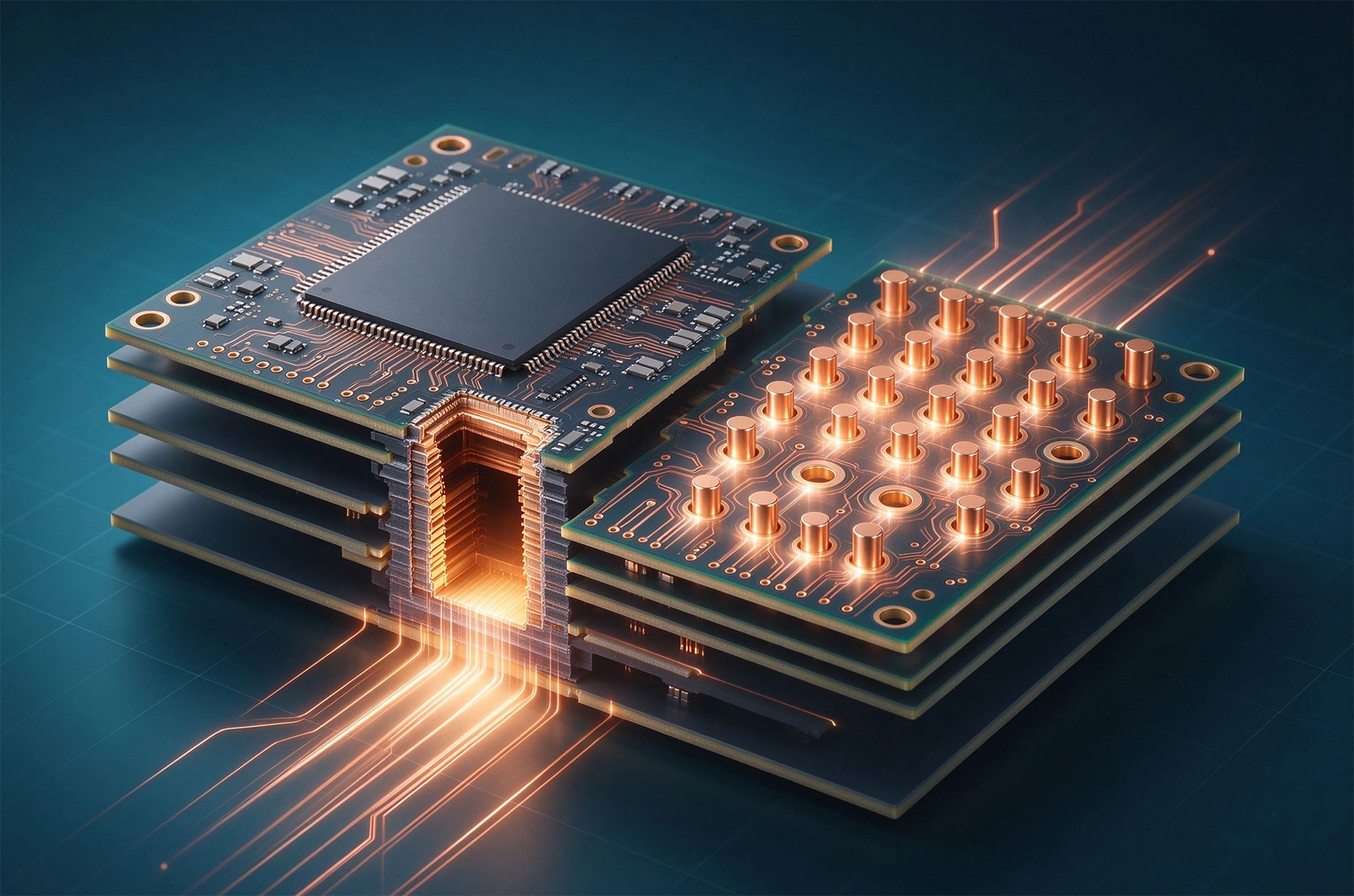
A blind via connects an outer layer to one or more inner layers without traversing the entire board thickness. This is in contrast to through-hole vias, which connect all layers from one outer surface to the other. Blind vias are manufactured using sequential lamination: the board is built up in stages, with certain layers being drilled and plated after specific lamination steps. The result is a via that is visible from one side of the board but terminates internally, which can be extremely useful for routing high-density power and signal interconnects without consuming valuable surface area.
In high-current applications, blind vias gain importance because they allow the designer to route heavy current paths through the most appropriate layers of the stackup. A power plane on layer two of a four-layer board might need to connect to components on the top layer. A blind via from the top layer to layer two provides that connection without the full-depth plating challenges of a through-hole that would also connect to layers three and four unnecessarily. This targeted connectivity improves Current Distribution and can reduce impedance in the power path.
The Current Carrying Capacity of a via is determined primarily by its barrel diameter, the thickness of the plating inside the barrel, and the thermal environment surrounding the via. Larger barrel diameters provide more cross-sectional copper area, which directly increases current capacity. Thicker copper plating, which is a standard option in most PCB Fabrication shops, multiplies that capacity further. Thermal relief in the surrounding copper plane affects how efficiently heat is conducted away from the via, which influences the allowable current before the via temperature rises to an unacceptable level.
Blind vias are expensive relative to through-hole vias. This is not because the concept is inherently complex but because the sequential lamination process required to produce them adds steps to the manufacturing workflow. A standard four-layer through-hole board requires drilling through the fully laminated stack, plating the holes, and then processing the result. A board with blind vias to internal layers requires drilling and plating at intermediate stages of the lamination sequence, which adds handling steps, additional process controls, and potential yield risk.
The cost premium for blind vias varies significantly by manufacturer and by the specific blind via configuration. A single blind via from layer one to layer two on a four-layer board might add only a modest cost increment. Multiple blind via structures, or blind vias that reach deeper into the stackup, can increase the board price by 30 to 50 percent or more depending on the complexity. This cost is why design decisions about via placement and current routing have direct financial consequences.
One of the key trade-offs in blind via design is the choice between using one large blind via and using multiple smaller blind vias to carry the same current. A single large blind via might require a drill size that approaches the manufacturing limit for the blind via process, increasing cost and potentially limiting the manufacturers who can produce it reliably. Multiple smaller vias distribute the current and can be fabricated with more standard equipment, but they consume more routing space and may require more complex fanout patterns that themselves add cost in signal routing density.
Pcb Design Standards such as Ipc-2152 provide guidance on current carrying capacity for traces and vias, but these standards are conservative by design and often pessimistic for Power Electronics applications where some temperature rise above ambient is acceptable. In practice, engineers working with power boards develop their own empirically validated guidelines based on the specific materials, stackup, and thermal environment of their application.
For blind vias in high-current applications, the critical parameters are barrel cross-sectional area, plating thickness, and thermal connectivity to adjacent copper planes. A blind via with 20 mil barrel diameter and one ounce copper plating has significantly more current carrying capacity than the same diameter with half-ounce plating, but it also costs more because the plating process takes longer and requires tighter process control. The designer must decide whether the incremental current capacity justifies the incremental cost.
Thermal simulation has become an practical tool for evaluating Via Current Capacity during the design phase. Finite element Thermal Analysis can model the temperature rise in a via structure under specified current loading, accounting for the thermal conductivity of the dielectric materials, the presence or absence of thermal relief in adjacent planes, and the effect of forced airflow or natural convection cooling at the board surface. While not every design warrants this level of analysis, it is increasingly accessible through EDA tool integrations and is worth using for high-current designs where via temperature is a concern.
Heavy Copper is one of the most effective ways to increase Via Current Capacity without changing the via geometry. Standard PCB Fabrication uses one ounce copper plating as a baseline. Increasing to two ounce, three ounce, or even heavier copper plating dramatically increases the cross-sectional area of the via barrel, which in turn increases the allowable current. For a blind via carrying 10 amperes or more, heavy copper plating is often the most practical path to meeting current requirements without resorting to exotic or expensive via structures.
The Manufacturing Cost of heavy copper plating is higher than standard plating because the process takes longer and requires more copper. However, the incremental cost is generally lower than the cost of adding additional via structures to share the current load, because those additional vias consume routing space and require more complex fanout routing that may force a larger board. When evaluating the cost trade-off, it is important to consider the total system cost, not just the per-via fabrication cost.
Blind vias with heavy copper plating are at the upper end of the manufacturing complexity spectrum. Not all PCB shops can produce them reliably, and those that can typically charge a premium. The combination of sequential lamination for the blind via structure and heavy copper plating for current capacity is a specialized capability. Engineering teams working on power electronics should identify capable manufacturers early in the design process and involve them in discussions about feasible plating weights and blind via depth combinations before finalizing the stackup design.
The board stackup is the foundation on which all subsequent via design decisions rest. A well-designed stackup for a high-current application allocates specific layers for Power Distribution, selects appropriate dielectric thicknesses to support the required voltage isolation, and positions the power layers at depths that are accessible to blind vias from the component layers where current enters and exits the board.
For a typical four-layer board with high-current requirements, a common configuration places Power Planes on layer two and three, with signal layers on the outer surfaces. Blind vias from the top layer to the internal Power Planes carry current from surface-mounted components to the internal distribution network. If the current magnitude is extreme, the designer may use filled or cap-plated blind vias to increase effective conductivity and improve thermal performance at the pad interface.
Stackup planning should also consider voltage isolation requirements between current-carrying layers and adjacent signal layers. High-current paths generate magnetic fields that can induce noise in nearby signal traces. Maintaining adequate separation or using ground shielding between power and high-speed signal layers is an important consideration that goes beyond simple current capacity calculations.
The most cost-effective approach to high-current blind via design is to minimize the number of blind via structures required. This is accomplished through thoughtful routing that consolidates high-current paths before they need to transition between layers, rather than routing individual component currents through separate via structures. A power path that aggregates currents from multiple components onto a wide trace before crossing a layer boundary can use one larger blind via instead of several smaller ones.
Where multiple via structures are unavoidable, using standard drill sizes as much as possible reduces Manufacturing Cost. Most PCB shops have optimized their blind via drilling process for a range of standard drill sizes, and designs that stay within those ranges benefit from better pricing and faster lead times. Custom drill sizes, while sometimes necessary for extreme current requirements, should be reserved for cases where standard sizes genuinely cannot meet the performance requirement.
Another practical strategy is to use blind vias only where they are genuinely needed for routing, and to use through-hole vias elsewhere. Through-hole vias are the lowest-cost option and can carry substantial current if properly sized and plated. A design that uses blind vias selectively for layer transitions that cannot be accomplished with through-holes, and relies on through-hole vias for the majority of layer connections, achieves the routing density benefit of blind vias while keeping manufacturing costs manageable.
Before finalizing a blind via design for a high-current application, it is advisable to consult with your PCB manufacturer early in the design cycle. Blind via capabilities vary widely between shops, and the specifications a manufacturer can reliably achieve may differ from what a datasheet suggests is possible. Parameters like the minimum blind via diameter, the maximum blind via depth, the achievable plating thickness in blind vias, and the flatness and registration tolerances of the finished board all depend on the specific equipment and process controls of the manufacturer.
When discussing a high-current blind via design with a manufacturer, be specific about current requirements and thermal constraints. Ask them to confirm achievable plating weights for the blind via structure you are considering, and request feedback on the drill size and depth combination you are planning. A manufacturer who regularly produces blind vias for power applications will have useful insights about process limitations that are not documented in general capability tables.
It is also worth asking about filled and cap-plated blind vias. Filled vias, where the barrel is filled with non-conductive or conductive material after plating, can improve thermal performance and provide a flat surface for component mounting. Cap plating, where additional copper is plated over the filled via to create a fully flat surface, is often used for BGA escape routing but can also benefit high-current applications by providing a larger contact area at the pad interface. These options add process steps and cost, but they may enable a more efficient overall design that justifies the investment.
High-current blind via design is an exercise in balancing competing priorities: current carrying capacity, thermal performance, manufacturing cost, and routing flexibility. The most effective designs approach this balance systematically, starting with a clear understanding of current requirements, selecting a stackup that supports efficient Power Distribution, and then making via design choices that meet the technical requirements at the lowest feasible manufacturing cost.
The key principles are straightforward: use heavy copper plating to maximize the capacity of existing via structures before adding more vias, minimize the number of blind via structures through thoughtful power routing, stay within standard manufacturing capabilities whenever possible, and engage your PCB manufacturer early in the design process to confirm feasibility and identify cost-saving opportunities. These practices will produce designs that perform reliably under high-current load while keeping manufacturing costs aligned with the project budget.
Contact us to discuss your requirements.
High Current PCB Silkscreen: Clearance Requirements for Heavy CopperOctober/23/2026

High Current PCB EMI Shielding: Ground Pour vs. Shielding CansAugust/14/2026
High Current PCB Solder Joints: Wave Soldering vs. Selective SolderingJuly/15/2026
Best Material for High Current PCB DesignMay/21/2026
High Current PCB Conformal Coating: Protecting Solder Joints Under Thermal StressAugust/06/2026
Best Material for High Current PCB Design: How to Choose the Right SubstrateJune/05/2026
High Current PCB Material Showdown: FR4 vs. Metal-Core vs. PolyimideJuly/14/2026
How Much Current Can a PCB Trace Carry? Complete Engineering GuideMay/20/2026