

Power Distribution in multilayer PCBs presents design challenges that differ fundamentally from signal-integrity-focused boards. When your design must carry significant current—tens of amps or more—the choices you make about layer arrangement, plane geometry, and stackup symmetry directly determine whether your board stays cool under load or slowly cooks itself into failure.
The symmetrical versus asymmetrical debate matters more in power applications than almost anywhere else in Pcb Design. The asymmetry you might tolerate in a pure signal board can create thermal gradients, mechanical warpage, and Current Density problems that silently degrade reliability in power designs.
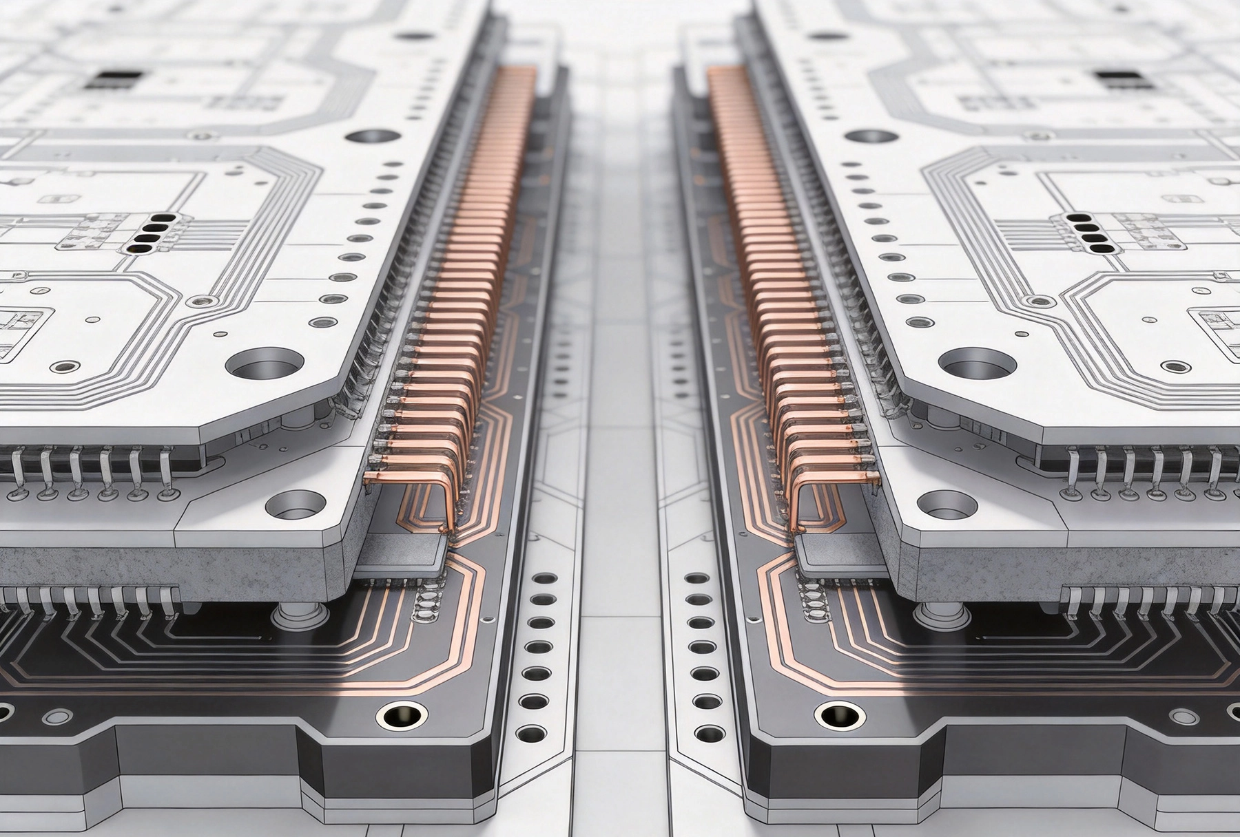
Before comparing stackup strategies, understanding how current actually flows through copper planes matters. Current doesn't distribute uniformly across a plane. It follows the path of lowest impedance, which means it crowds near plane edges, around apertures, and through narrowing neck-downs created by component pads and via antipads.
In High Current applications, this non-uniform distribution creates hot spots. A 20-amp design with poor plane geometry can concentrate that current through a path with only a fraction of the intended cross-section, pushing Current Density through the roof at specific points. Managing this distribution requires deliberate plane design that goes beyond simple copper area calculations.
Power planes also serve as heat spreaders. The copper itself conducts heat away from component hotspots, and the plane geometry determines how effectively that heat distributes across the board surface. A poorly designed power plane might technically have sufficient copper area for current, but create localized temperatures that exceed component ratings.
Symmetrical stackup refers to the arrangement of dielectrics and copper layers mirrored around the board's centerline. A simple four-layer symmetric stackup might look like: signal layer, prepreg, ground plane, core, power plane, prepreg, signal layer. The dielectric thicknesses above and below each internal plane are equal.
This symmetry provides mechanical balance. During lamination, the pressures and temperatures that shape the board affect each side equally. The result is flat boards with minimal warpage—important for assembly processes and for maintaining reliable via connections over thermal cycles.
For High Current designs, symmetric stackup offers some advantages. When power and ground planes occupy symmetric positions relative to the board center, their thermal expansion is better controlled. The mechanical stability also helps with Plated Through-hole reliability in Thermal Cycling environments.
However, pure symmetry can limit your options for Current Distribution. In a standard symmetric stackup, power and ground planes are often paired as adjacent layers. This works well for controlled impedance but forces all your high-current paths into the same layer pair, constraining your routing flexibility.
Asymmetrical stackup means the dielectric thicknesses above and below key planes differ. You might place your main power plane on layer three with a thin dielectric to the layer above and a thick dielectric to the layer below. This creates an intentionally unbalanced structure.
Asymmetry becomes attractive in high current designs when you need to spread current across multiple layer pairs. By separating power planes onto non-adjacent layers, you create multiple parallel current paths. If your design carries 30 amps, distributing that across two 4-ounce copper planes rather than one 8-ounce plane can simplify manufacturing while improving Current Distribution.
Thermal Management benefits drive many asymmetrical choices. Placing a power plane closer to the PCB surface with a thin dielectric allows heat to transfer more effectively to the surface and into any attached heatsinks or thermal pads. The asymmetric arrangement lets you optimize for thermal performance rather than mechanical symmetry.
Component Placement flexibility also increases with asymmetry. When power planes aren't constrained to symmetric positions, you can route high-current traces on multiple layers and connect them with Thermal Vias, creating current distribution networks that would be impossible in a strictly symmetric arrangement.
High current designs fail thermally before they fail electrically in most cases. A trace rated for 10 amps might pass electrical testing while creating hotspots that accelerate surrounding component aging or cause solder joint fatigue over time.
Symmetric stackups spread heat more uniformly due to their balanced structure. The thermal gradients across symmetric boards tend to be gradual and predictable. This predictability simplifies thermal modeling and helps you design appropriate margins into your Power Distribution network.
Asymmetric designs require more careful Thermal Analysis because heat distribution becomes less predictable. A power plane near the surface with thin dielectric will dump heat into that surface layer more aggressively than a buried plane. If your board operates in an enclosure, this localized heating can create temperature gradients that affect components far from the heat sources.
The practical approach for asymmetric power designs often involves adding dedicated thermal relief vias, spreading copper pours in surface layers, and incorporating thermal simulation into the design process. These additions compensate for the less predictable heat distribution that asymmetry introduces.
Pcb Warpage becomes more than an aesthetic concern in high current applications. Warped boards cause uneven solder paste deposition, inconsistent reflow profiles, and stressed component leads. For boards operating with Thermal Cycling, warpage-induced stress concentrates at via barrels and plated through-holes—exactly the structures carrying your high current.
Symmetric stackups resist warpage because their balanced construction equalizes internal stresses from thermal expansion. During assembly reflow, a symmetric board maintains flatness more reliably than an asymmetric board of equivalent complexity. This flatness translates directly to assembly yield and long-term reliability.
Asymmetric designs require compensation strategies. Some designers specify heavier copper on one side to balance mechanical forces. Others incorporate metal core or Heavy Copper backbars that constrain warpage. The manufacturing process itself may need adjustment—longer press cycles, lower temperature ramps, or specialized tooling that holds the board flat during lamination.
For production volumes, asymmetric high-current boards often justify the extra manufacturing attention because the electrical and thermal benefits outweigh the added process complexity. For prototypes or low-volume runs, the extra cost of warpage compensation might not pencil out.
Regardless of stackup symmetry choice, vias in high current paths demand special treatment. Standard through-hole vias with typical barrel plating can't reliably carry the current that surface traces handle. Thermal relief and via sizing become critical design decisions.
In symmetric stackups, current can distribute across vias on multiple layers if you use buried or blind vias strategically. A design might route power through layer one, down through Thermal Vias to an internal plane, across that plane, and back up through another set of thermal vias. The symmetric arrangement makes these transitions predictable and easier to model.
Asymmetric arrangements require even more attention to via current sharing. When power planes occupy non-adjacent layers, current must travel through via barrels that may have thermal gradients along their length. Filled and capped vias become important for ensuring reliable current conduction without hot spots at the layer transitions.
Current derating for vias isn't optional in High Current Design. Industry guidelines typically derate Via Current Capacity by 30-50% compared to equivalent trace width. If your calculation says you need a via that handles 5 amps, specifying a via rated for 7-10 amps with appropriate thermal relief provides the margin necessary for long-term reliability.
Heavy Copper and asymmetric stackups push manufacturing capabilities. A board with 4-ounce copper on internal planes and 2-ounce copper on surfaces requires different processing than standard boards, and not every fabricator handles these requirements equally well.
Symmetric designs with heavy copper are generally more universally manufacturable. The balanced construction doesn't challenge standard lamination processes as severely, and most capable fabricators have established parameters for symmetric heavy-copper boards. If your priority is finding a wide range of manufacturing sources, symmetric stackups offer more flexibility.
Asymmetric heavy-copper boards often require specialized manufacturers with experience in non-standard constructions. The lamination process must compensate for differential expansion between thick and thin sections. Drill and plating processes may need multiple steps to achieve reliable barrel plating in boards with extreme thickness variations between layers.
Building a relationship with a fabricator experienced in your specific stackup type pays dividends that go beyond initial pricing. Those manufacturers can advise on design rules that account for their specific process capabilities, catch potential problems during DFM review, and suggest optimizations that improve both yield and reliability.
Symmetric stackups make sense when your design priorities favor predictability and wide manufacturing access. If you're working with standard copper weights, need to minimize development time with multiple fabrication sources, or operate in thermally challenging environments where mechanical stability matters most, symmetric construction provides a solid foundation.
Asymmetric stackups become the better choice when thermal performance drives the design, when you need to distribute current across multiple parallel planes, or when Component Placement constraints make symmetric routing impractical. The added manufacturing complexity often pays back through improved electrical performance and thermal margins.
Hybrid approaches exist and often work best. You might specify a primarily symmetric stackup but incorporate strategic asymmetry in specific layer pairs where thermal or current distribution needs are highest. This approach captures some benefits of each strategy while keeping manufacturing complexity manageable.
No amount of simulation replaces physical testing for high current designs. Thermal imaging during operation reveals hot spots that calculations miss. Current distribution measurements across parallel paths confirm that your design actually behaves as modeled.
Accelerated life testing under worst-case thermal conditions catches reliability issues before they manifest in the field. Cycling the board between temperature extremes while monitoring for opens or increased resistance identifies failure modes that might not appear in room-temperature testing.
Cross-section analysis of via structures and layer interfaces provides confidence that the physical board matches your design intent. This destructive testing reveals plating quality, lamination integrity, and any delamination that could compromise current paths under thermal stress.
High Current PCB layer stackup design requires balancing electrical, thermal, and mechanical considerations that interact in complex ways. Symmetric stackups provide predictable behavior and easier manufacturing but constrain your options for current distribution and Thermal Management. Asymmetric arrangements unlock performance benefits but demand more careful analysis, specialized manufacturing relationships, and thorough validation.
The choice ultimately depends on your specific design priorities. For most high-current applications, I recommend starting with symmetric construction unless thermal performance requirements clearly justify asymmetry. The manufacturing simplicity and design predictability provide a solid foundation that you can optimize with asymmetric elements where they provide measurable benefit.
Whatever stackup strategy you choose, invest in thorough thermal modeling, realistic load testing, and appropriate derating for vias and traces. The extra engineering time spent validating your stackup decision pays back through reliable products that perform consistently throughout their operational life.
High Current PCB Embedded Copper: Internal vs. External Heat DissipationSeptember/26/2026
Cost Comparison: 2oz vs 4oz Copper PCB — What You Need to KnowJune/26/2026
High Current PCB Mounting Holes: Plated vs. Non-Plated for Current ReturnSeptember/29/2026
High Current PCB Design for Railway Traction SystemsAugust/07/2026
High Current PCB Design for Industrial Motor DrivesSeptember/28/2026
High Current PCB Material Showdown: FR4 vs. Metal-Core vs. PolyimideJuly/14/2026
High Current PCB Current Sensing: Shunt Resistor vs. Hall Effect LayoutJuly/29/2026
High Current PCB Design for Drone ESCs: Minimizing Loop InductanceAugust/03/2026