Home Blog High Current PCB Thermal & Design

High Current PCB Design for Electric Vehicle Charging Stations

August/15/2026

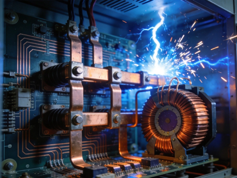
The rapid growth of electric vehicle adoption has created unprecedented demand for reliable, high-power charging infrastructure. At the heart of every EV charging station lies a sophisticated Power Electronics system, with printed circuit boards serving as the critical foundation for power conversion, control, and safety functions. Designing PCBs capable of handling the high currents required for Level 2 and DC fast charging presents unique engineering challenges that differ significantly from conventional electronics design.

EV charging stations must deliver power ranging from 7 kW for residential Level 2 chargers to 350 kW or more for commercial DC fast charging stations. These power levels require careful attention to Current Carrying Capacity, Thermal Management, electromagnetic compatibility, and safety isolation. This comprehensive guide explores the essential design considerations for creating robust, reliable high-current PCBs for EV charging applications.
High Current PCB Design for Electric Vehicle Charging Stations

Understanding EV Charging Power Requirements

Charging Levels and Power Profiles

Before diving into Pcb Design specifics, it's essential to understand the power requirements that define EV charging infrastructure:

  • Level 1 Charging (AC) – 120V, up to 1.9 kW, standard residential outlets
  • Level 2 Charging (AC) – 208-240V, 3-19 kW, dedicated residential and commercial installations
  • DC Fast Charging (DCFC) – 200-1000V, 50-350+ kW, commercial highway charging
  • Ultra-Fast Charging – Up to 1000 kW, emerging high-power charging standards

PCB designers must accommodate current flows ranging from 32A for basic Level 2 chargers to 500A or more for high-power DC fast charging stations. These current levels demand specialized approaches to trace sizing, component selection, and Thermal Management.

Key Design Challenges

High-current EV charging PCBs face several critical challenges:

  • Current Density management – Preventing excessive heating in traces and vias
  • Voltage isolation – Maintaining creepage and clearance distances for safety
  • Thermal Cycling – Surviving repeated temperature excursions during operation
  • Electromagnetic interference – Managing switching noise in power converters
  • Reliability requirements – Ensuring 10+ year operational life in harsh environments

Trace Sizing and Current Capacity

IPC-2152 Standard for High Current Design

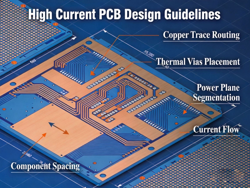
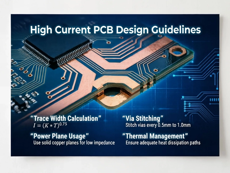
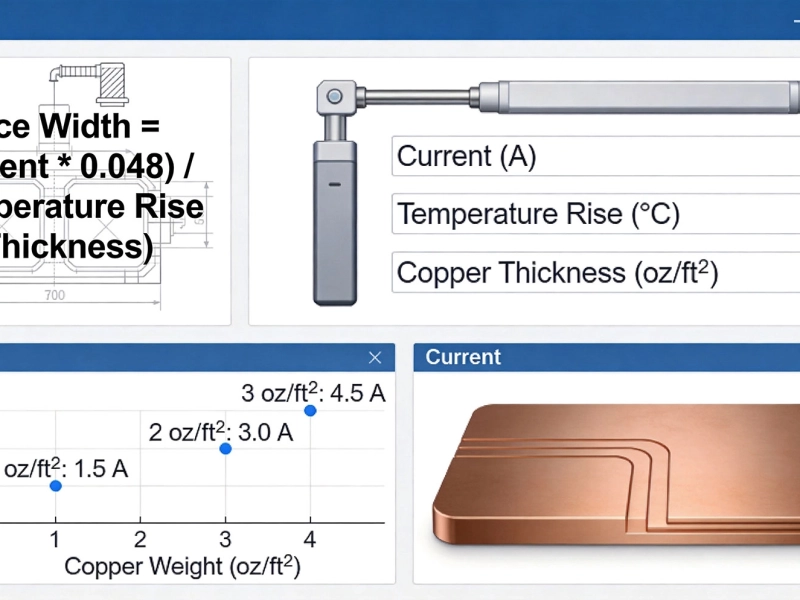
The Ipc-2152 standard provides the industry-accepted methodology for calculating trace width based on current capacity and acceptable temperature rise. Unlike the older Ipc-2221 Standard, Ipc-2152 accounts for modern PCB constructions and provides more accurate predictions for high-current applications.

Key factors affecting trace sizing include:

  • Current magnitude – Higher currents require wider traces or thicker copper
  • Acceptable temperature rise – Typically 10-20°C above ambient for reliable operation
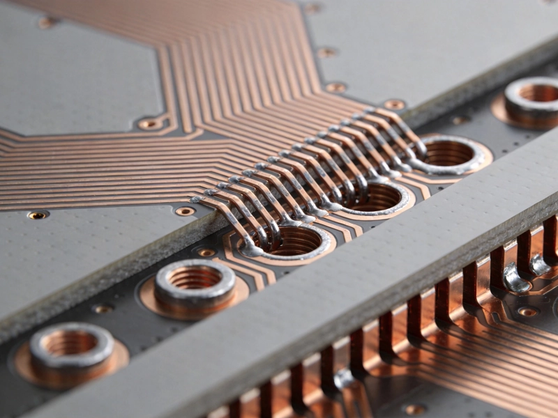
  • Copper Thickness – Heavy copper (2-20 oz) significantly increases current capacity
  • Trace length – Longer traces have higher resistance and greater heating
  • Environment – Ambient temperature and airflow affect cooling

Heavy Copper PCB Considerations

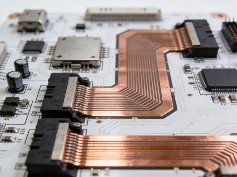
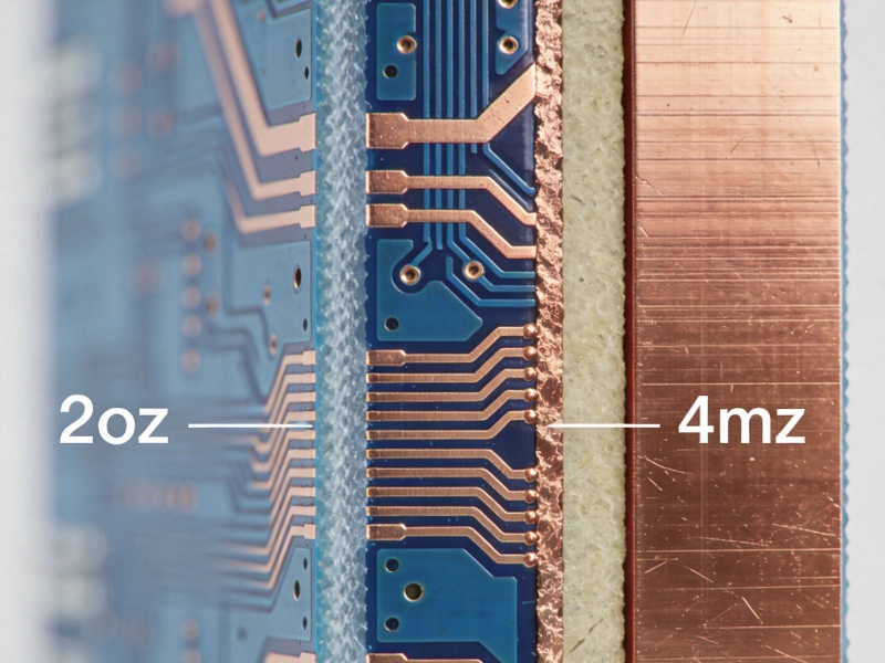
EV charging applications often require heavy copper PCBs with copper weights from 4 oz to 20 oz or more:

  • Current capacity – 6 oz copper can carry approximately 3x the current of 1 oz for the same width
  • Thermal performance – Thicker copper spreads heat more effectively
  • Mechanical strength – Heavy copper provides structural robustness for large components
  • Manufacturing constraints – Heavy copper requires specialized etching and plating processes

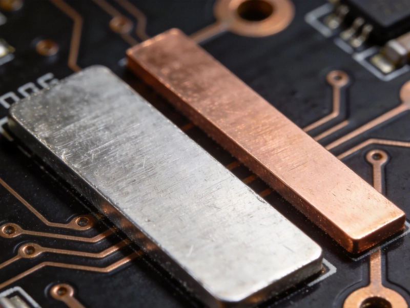
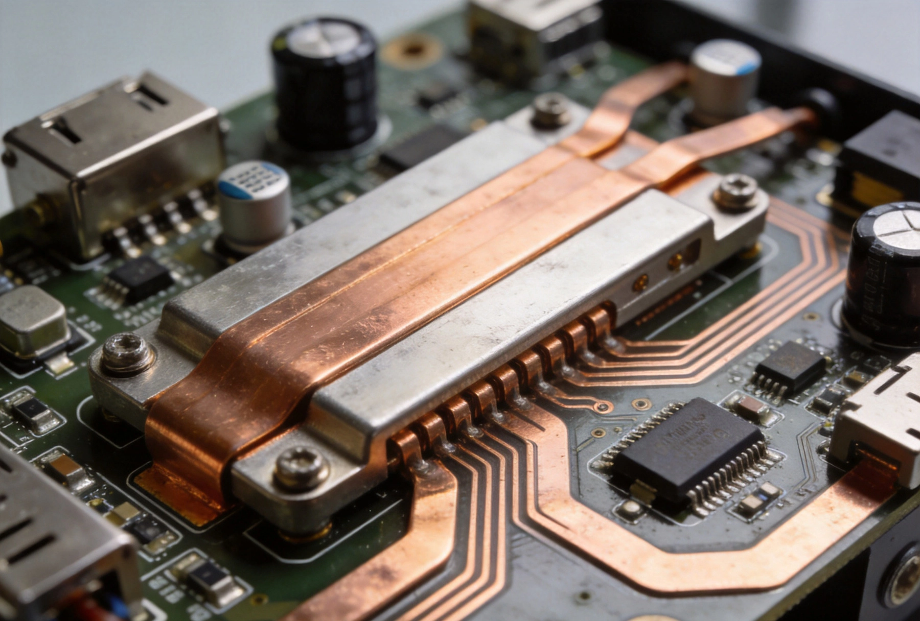
For very high currents, designers may use external bus bars soldered to the PCB, combining the advantages of PCB-based control electronics with the current capacity of discrete conductors.

Via Design for High Current

Vias represent bottlenecks in high-current paths. Proper via design requires:

  • Multiple parallel vias – Distributing current across many vias reduces heating
  • Increased via plating – Heavy copper plating (25-50 μm) improves current capacity
  • Thermal Vias – Connecting to internal copper planes for Heat Dissipation
  • Via filling – Conductive fill improves thermal conductivity and mechanical strength

As a general guideline, parallel vias should provide at least twice the copper cross-sectional area of the connected traces.

Thermal Management Strategies

Heat Generation in High Current PCBs

Power losses in high-current PCBs generate significant heat through several mechanisms:

  • I²R losses in traces – Resistive heating proportional to current squared
  • Switching losses – Power dissipation in MOSFETs and IGBTs
  • Conduction losses – Voltage drop across diodes and rectifiers
  • Magnetic losses – Core heating in inductors and transformers

Effective thermal management prevents excessive temperatures that degrade reliability and can trigger protection shutdowns.

PCB-Based Thermal Solutions

Several Pcb Design techniques enhance thermal performance:

  • Copper pours and planes – Large copper areas spread heat away from hot spots
  • Thermal Vias – Conduct heat to internal copper layers and opposite board surfaces
  • Metal core substrates – Aluminum or copper core PCBs provide excellent heat spreading
  • Thick copper layers – Heavy outer layers (4-10 oz) improve heat conduction
  • Direct bond copper – Ceramic substrates with bonded copper for extreme thermal requirements

External Cooling Integration

High-power EV charging PCBs typically require active cooling:

  • Forced air cooling – Fans directing airflow across hot components and PCB surfaces
  • Liquid cooling – Cold plates contacting thermally critical PCB areas
  • Heat Sinks – Aluminum extrusions attached to power devices and copper planes
  • Phase change materials – Thermal interface materials improving contact conductivity

Thermal simulation using computational fluid dynamics (CFD) helps optimize cooling system design before prototyping.

Component Selection for High Current

Power Semiconductors

EV charging applications demand power semiconductors capable of handling high currents and voltages:

  • Silicon Carbide (SiC) MOSFETs – Higher efficiency, faster switching, better thermal performance than silicon
  • IGBTs – Cost-effective for very High Current applications
  • GaN devices – Emerging technology for high-frequency, high-efficiency converters
  • Power modules – Integrated multiple dies with optimized thermal interfaces

Component selection balances efficiency, cost, switching frequency, and thermal requirements.

Capacitors for High Current

Capacitor selection significantly affects reliability in high-current applications:

  • Electrolytic capacitors – High capacitance values for bulk energy storage
  • Film capacitors – Excellent for high ripple current and long life
  • Ceramic capacitors – Low ESR for high-frequency decoupling
  • Aluminum polymer capacitors – Lower ESR than conventional electrolytics

Ripple current ratings must account for actual operating conditions, including frequency and temperature.

Magnetic Components

Inductors and transformers in EV charging applications handle substantial power:

  • Core material selection – Ferrite, powdered iron, or amorphous materials based on frequency
  • Conductor sizing – Litz wire or foil windings for high currents
  • Thermal management – Core and winding losses require effective heat removal
  • Isolation requirements – Safety-rated insulation for grid-connected applications

Safety and Isolation Design

Creepage and Clearance Requirements

EV charging stations connect to high-voltage AC mains and deliver dangerous voltage levels to vehicle connections. Safety standards mandate specific spacing requirements:

  • Creepage distance – Along surface path between conductors of different potentials
  • Clearance distance – Shortest air path between conductors
  • Working voltage – Determines required spacing based on insulation coordination
  • Pollution degree – Environmental contamination affects creepage requirements

IEC 61851 and UL 2202 define specific requirements for EV charging equipment, with spacing requirements varying from 2.5mm for low-voltage circuits to 25mm or more for high-voltage isolation barriers.

Reinforced Isolation

Control circuits often require reinforced isolation from high-voltage power sections:

  • Optocouplers – Optical isolation for feedback and control signals
  • Digital isolators – Capacitive or magnetic isolation for high-speed communication
  • Isolation amplifiers – Signal conditioning across isolation barriers
  • Gate drivers – Isolated drivers for power semiconductor control

Isolation components must meet safety standards for working voltage and transient overvoltage ratings.

Protective Features

Comprehensive protection ensures safe operation under fault conditions:

  • Overcurrent protection – Current sensing and rapid shutdown capability
  • Overvoltage protection – Surge suppression and voltage clamping
  • Overtemperature protection – Thermal monitoring and derating
  • Ground fault protection – Detection of unintended current paths
  • Arc fault detection – Identifying dangerous arcing conditions

Electromagnetic Compatibility

EMI Challenges in EV Chargers

Switching power converters in EV charging stations generate significant electromagnetic interference:

  • Conducted emissions – Noise coupled onto power lines
  • Radiated emissions – Electromagnetic radiation from switching loops
  • Common mode noise – Noise appearing equally on multiple conductors
  • Differential mode noise – Noise between power conductors

CISPR 11 and FCC Part 15 define emission limits for EV charging equipment.

PCB Layout for EMI Reduction

Proper layout minimizes EMI generation and coupling:

  • Minimize switching loops – Keep high di/dt paths as small as possible
  • Shielding planes – Ground planes beneath switching circuits
  • Filtering – Input and output filters for conducted noise
  • Separation – Physical spacing between noisy and sensitive circuits
  • Symmetry – Balanced layouts for common mode cancellation

Reliability and Environmental Considerations

Environmental Stress Factors

EV charging stations operate in challenging environments:

  • Temperature extremes – -40°C to +50°C ambient operation
  • Humidity – High humidity and condensation in outdoor installations
  • Vibration – Transportation and installation stress
  • Pollution – Dust, salt, and chemical contamination
  • UV exposure – Sunlight degradation of materials

Material Selection for Harsh Environments

PCB materials must withstand environmental stressors:

  • High Tg laminates – Glass transition temperature above 170°C for thermal stability
  • Low CTE materials – Minimizing thermal expansion stress on heavy components
  • Conformal coating – Protection against moisture and contamination
  • Potting compounds – Encapsulation for extreme environmental protection

Thermal Cycling Reliability

Repeated heating and cooling creates mechanical stress:

  • CTE matching – Selecting materials with compatible expansion coefficients
  • Component mounting – Secure attachment for heavy components
  • Via reliability – Avoiding via cracking through proper design
  • Solder joint integrity – Adequate solder volume and thermal relief

Design Verification and Testing

Electrical Testing

Comprehensive testing validates design performance:

  • Hi-pot testing – Verification of isolation barriers
  • Insulation resistance – Confirming adequate insulation performance
  • Continuity testing – Verifying high-current path integrity
  • Thermal imaging – Identifying hot spots during operation

Environmental Testing

Qualification testing ensures reliability:

  • Temperature cycling – Validating thermal expansion management
  • Thermal shock – Rapid temperature change survival
  • Humidity testing – Moisture resistance validation
  • Vibration and mechanical shock – Transportation and installation robustness

Conclusion

High Current Pcb Design for EV charging stations represents a specialized discipline requiring careful attention to thermal management, safety isolation, and electromagnetic compatibility. Success demands mastery of Heavy Copper Pcb technologies, power semiconductor applications, and harsh environment reliability engineering.

As EV charging power levels continue increasing to reduce charging times, the engineering challenges become more demanding. Designers must balance efficiency, cost, reliability, and safety while pushing the boundaries of power density. By applying the principles outlined in this guide—proper trace sizing, effective thermal management, comprehensive safety features, and rigorous environmental design—engineers can create EV charging solutions that meet the demanding requirements of this rapidly growing market.

The transition to electric transportation depends on reliable, ubiquitous charging infrastructure. High-quality PCB design is fundamental to delivering charging stations that provide safe, efficient, and dependable service for the decade-long lifespans required in this critical application.

Expert High Current PCB Design Services

Our engineering team specializes in high-power PCB designs for EV charging and industrial applications. From heavy copper layouts to thermal management solutions, we deliver reliable designs that meet the most demanding requirements. Contact us to discuss your High Current Pcb project.

Frequently Asked Questions

What copper weight is recommended for EV charging PCBs?

EV charging PCBs typically use 4-10 oz copper for power paths, with some high-current applications requiring up to 20 oz. The specific requirement depends on current magnitude, thermal constraints, and available board space.

How do I calculate trace width for high current applications?

Use the IPC-2152 standard for accurate calculations, considering current magnitude, acceptable temperature rise, Copper Thickness, and environmental conditions. Online calculators based on IPC-2152 provide good starting points, but thermal validation testing is recommended.

What safety standards apply to EV charging station PCBs?

Key standards include IEC 61851 (EV conductive charging systems), UL 2202 (EV charging system equipment), IEC 61439 (low-voltage switchgear), and various EMC standards including CISPR 11 and FCC Part 15.

Is liquid cooling necessary for EV charging PCBs?

Cooling requirements depend on power level and design efficiency. Level 2 chargers often use air cooling, while high-power DC fast chargers typically require liquid cooling to manage heat from power semiconductors and magnetics.

What PCB materials work best for high current EV applications?

High Tg FR-4 (170°C+) works for many applications, while extreme power levels may require ceramic-based substrates (DBC, DBA) or metal core PCBs for optimal thermal performance. Material selection balances thermal requirements, cost, and manufacturing complexity.
Send Message
Name*
E-mail*
Country*
Phone/WhatsApp*
Name*
E-mail*
Country*
Phone/WhatsApp*