

When designing high-speed or high-current digital circuits, decoupling capacitors are your first line of defense against Power Integrity failures. But when the currents involved reach the ampere level -- think FPGA I/O banks, high-performance microcontrollers, RF transceivers, or high-speed SerDes lanes -- the difference between a well-behaved power rail and a catastrophically noisy one often comes down to two geometric parameters: placement distance and loop area. This article explores why these two factors matter, how they interact, and what practical rules you can follow to get them right.
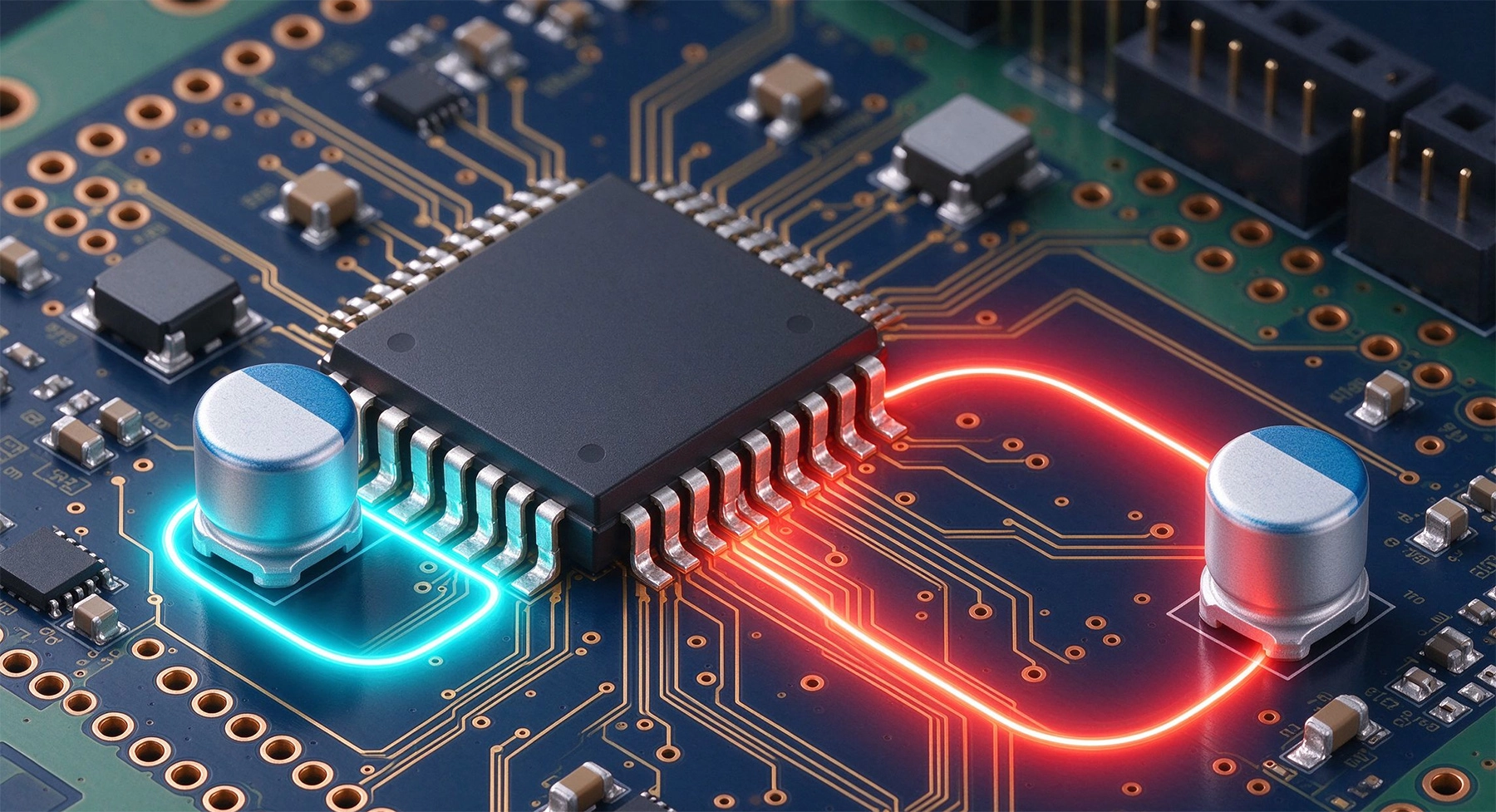
Decoupling capacitors serve a deceptively simple purpose: they provide a local reservoir of charge that can be discharged into the IC within nanoseconds, compensating for the finite impedance of the Power Distribution network (PDN). At low currents, the parasitic inductance of the capacitor's mounting path is tolerable -- the voltage droop it causes is small enough to stay within the IC's noise margin.
But when an IC draws a step current of several amperes with sub-nanosecond rise times, even a few nanohenries of parasitic inductance can generate a voltage spike of hundreds of millivolts (V = L x di/dt). That spike can cause logic errors, timing jitter, or outright latch-up. The key insight is this: the capacitor's effectiveness is not determined by its capacitance value alone -- it is determined by how quickly that capacitance can deliver current to the IC, which is a function of the parasitic Loop Inductance.
Placement distance refers to the physical separation between the decoupling capacitor and the IC's power supply pins. In Pcb Layout terms, it is the length of the trace (or via) connecting the capacitor pad to the IC pin. The shorter this distance, the lower the parasitic inductance of the connection, and the more effective the capacitor is at high frequencies.
A useful rule of thumb is that a 1 mm long, 6 mil wide trace on a standard FR4 PCB contributes approximately 0.5 nH of series inductance. A via adds roughly 0.8-1.2 nH. So a capacitor placed 5 mm away from the IC pin, connected by two vias and a short trace, can easily add 3-4 nH of parasitic inductance -- enough to render a 100 nF capacitor ineffective above 10 MHz.
On multi-layer boards, you can reduce placement distance further by using vertical transitions strategically:
Loop area is the physical area enclosed by the current path from the IC power pin, through the decoupling capacitor, and back to the IC ground pin. This is distinct from placement distance -- you can have a capacitor placed very close to the pin but still suffer from high Loop Inductance if the return path loops widely.
The parasitic inductance of a loop is directly proportional to its area: L = mu_0 x Area / Height, where Height is the distance between the signal layer and the reference ground plane. Doubling the loop area doubles the inductance.
For a rectangular loop formed by a trace and its return path on an adjacent ground plane, a practical approximation is:
L_loop (nH) = 5.08 x h x ln(4 x l / w)
Where h is the height of the trace above the reference plane, l is the loop length, and w is the trace width. This formula shows that reducing loop area (by shortening l and keeping h small) is critical.
A common mistake is to focus only on the connection from capacitor to power pin while neglecting the return path from capacitor to ground. The complete decoupling loop includes both the supply and return paths. If the ground connection is long or routed through a split plane, the loop area balloons and the capacitor's high-frequency performance collapses.
Best practice: Use via pairs -- one via from capacitor to power plane, another from capacitor to ground plane -- placed as close together as possible. The magnetic fields from the forward and return currents partially cancel, reducing effective loop inductance by 30-50% compared to a single via.
This is the central question of this article. The answer depends on frequency and current level, but here is a practical framework:
| Parameter | Primary Effect | Frequency Range Affected | Typical Inductance Contribution |
|---|---|---|---|
| Placement Distance | Series inductance of connection trace | Above ~10 MHz | ~0.5 nH per mm of trace |
| Loop Area | Total loop inductance (supply + return) | Above ~1 MHz | Proportional to enclosed area |
Key takeaway: Loop area dominates at lower frequencies (1-10 MHz range) where the loop perimeter becomes a significant fraction of the wavelength. Placement distance dominates at higher frequencies (>100 MHz) where the parasitic trace inductance directly limits the capacitor's self-resonant frequency effectiveness. For modern high-speed designs operating across both ranges, both parameters must be optimized simultaneously.
Consider a modern FPGA with 500+ I/O pins drawing peak currents of 5A with <1 ns rise times. The power delivery network might use:
Simulation results typically show that moving the 10 nF capacitor from 5 mm to 1 mm placement distance reduces the PDN impedance peak by 6-8 dB, while simultaneously minimizing the loop area (via pair spacing <0.5 mm) provides an additional 3-4 dB improvement. The combined effect can mean the difference between meeting and failing SI/PI specifications.
Beyond hand calculations, modern Pcb Design relies on electromagnetic simulation to validate decoupling strategies:
In high-current Pcb Design, decoupling capacitor placement is not just about picking the right capacitance value -- it is fundamentally a geometry problem. Placement distance controls the series parasitic inductance that limits high-frequency effectiveness, while loop area determines the total inductance of the current delivery path including the critical ground return.
The most effective decoupling strategy optimizes both parameters simultaneously: place capacitors as close as possible to IC power pins (short placement distance) and ensure the supply and return current paths form the smallest possible loop (minimal loop area). When combined with proper plane design, via stitching, and EM simulation validation, these techniques enable robust Power Integrity even in the most demanding high-current, high-speed applications.
Remember: a 100 nF capacitor placed poorly is worse than useless -- it can actively degrade your power integrity by introducing resonance peaks and excessive loop inductance. A 10 nF capacitor placed optimally, on the other hand, can deliver exceptional high-frequency decoupling performance. Place smart, loop tight, and your PDN will thank you.
High Current PCB Via Plating: 1mil vs. 2mil Thickness Reliability TestAugust/03/2026
IPC-2152 Current Carrying Capacity: The Definitive PCB Trace Calculator GuideMay/21/2026
High Current PCB Annular Rings: Minimum Size vs. Reinforced SizeAugust/12/2026
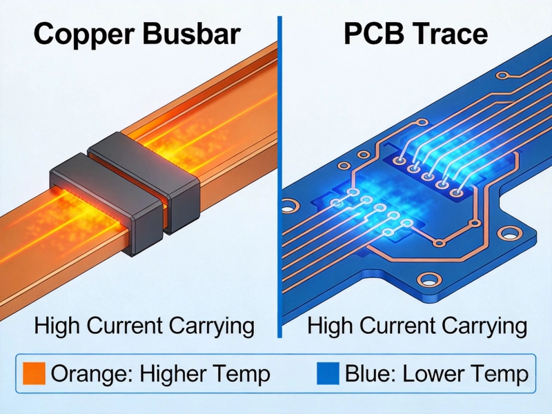
Bus Bar vs PCB Trace for High CurrentMay/21/2026
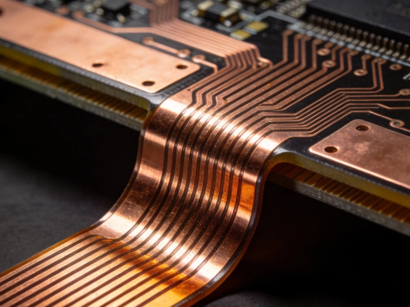
High Current PCB Flex-Rigid: Current Capacity in Bend AreasOctober/09/2026
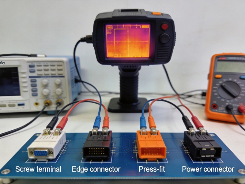
High Current PCB Connector Selection: Test Results and Real Performance DataMay/21/2026
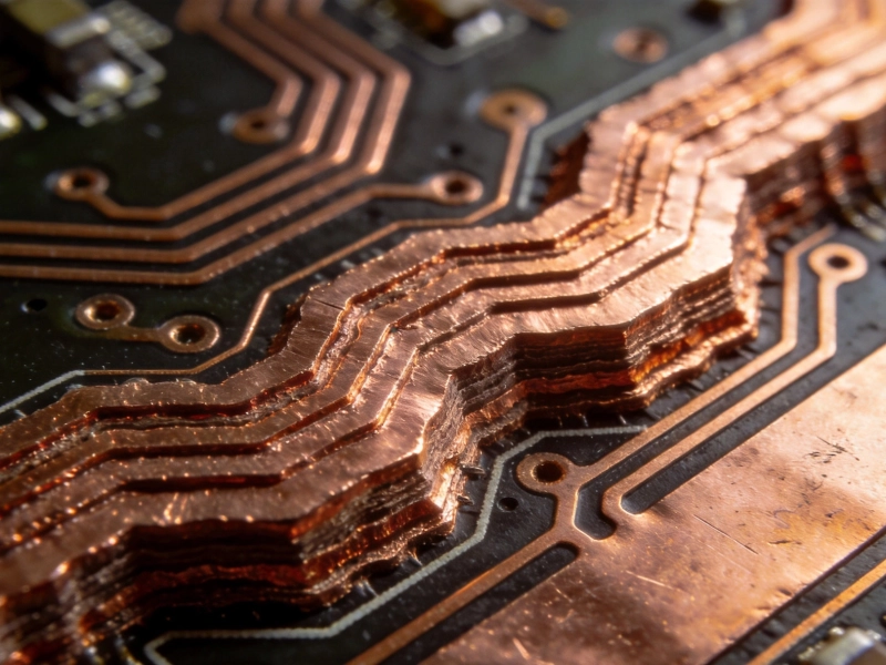
High Current PCB Bus Bars vs. Heavy Copper Traces: Cost and PerformanceJuly/25/2026
High Current PCB Testing: Thermal Imaging vs. 4-Wire Kelvin MeasurementJuly/22/2026