

Via plating thickness represents one of the most consequential specifications in High Current PCB design. When engineers design Power Distribution networks for automotive motor drives, industrial motor controllers, or server power supplies, the copper plating inside plated through-holes carries current between layers. The difference between 1mil and 2mil plating thickness significantly impacts Current Carrying Capacity, thermal performance, and long-term reliability. Making the right choice requires understanding how plating specifications interact with operating conditions and failure mechanisms.
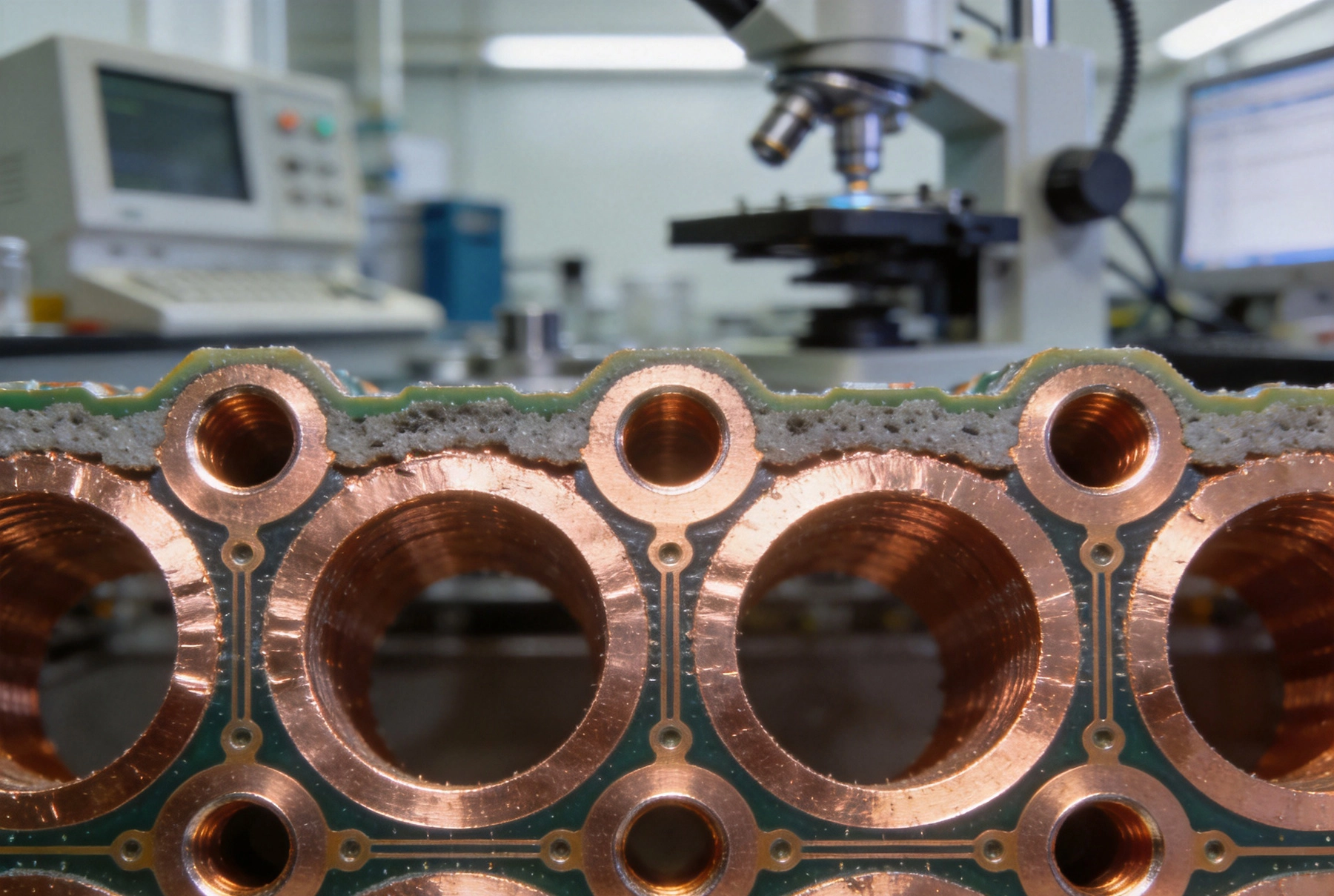
A plated through-hole connects conductive traces on different layers using copper electrodeposited onto the barrel walls. Standard PCB Fabrication typically produces 1mil (25 micrometers) plating thickness as the default specification. This thickness works adequately for signal routing where currents stay below fractions of an ampere, but power applications demand thicker plating to handle amperes or tens of amperes flowing through individual vias.
The copper inside a via barrel carries current along its inner surface, creating a cylindrical conductor. Current Density concentrates at the surface due to skin effect, becoming more pronounced at higher frequencies, though DC and low-frequency current distributes more uniformly across the cross-section. The effective current carrying area depends directly on plating thickness—doubling the plating from 1mil to 2mil approximately doubles the cross-sectional conductor area, though the relationship to current capacity involves thermal considerations as well.
Via reliability under High Current involves more than simple current capacity calculations. Temperature rise within the via barrel creates thermal stress that compounds with board-level Thermal Cycling. Vias that survive initial current stress testing might fail after thousands of thermal cycles as thermal expansion mismatch between copper and substrate gradually degrades the plating-to-barrel interface.
For a standard 12mil diameter through-hole, 1mil plating produces approximately 35 square mils of copper cross-section, while 2mil plating roughly doubles this to 69 square mils. This doubling does not directly translate to doubled current capacity because Thermal Management, not purely resistive heating, typically limits via current ratings. However, thicker plating reduces resistance, lowering I-squared-R heating at any given current level.
The resistance difference matters most at high currents. A via with 1mil plating might exhibit 2-3 milliohms of resistance, while 2mil plating reduces this to 1-1.5 milliohms. At 10 amperes, the power dissipation difference between these resistance values translates to approximately 100-150 milliwatts of additional heating in the thinner-plated via—heat that must dissipate through the surrounding dielectric material.
Standard PCB Fabrication processes easily achieve 1mil plating as a baseline specification. The process uses acid copper plating with organic additives that control grain structure and throwing power. Achieving consistent 1mil coverage across via walls with good adhesion represents established technology that most manufacturers deliver reliably.
2mil plating requires extended plating time and optimized process parameters. The longer electrodeposition cycle increases Manufacturing Cost and cycle time, typically adding 15-25 percent to fabrication pricing for boards specifying heavy plating. More importantly, achieving uniform 2mil thickness throughout the barrel requires process capability that not all manufacturers possess consistently. Surface roughness, voids, and adhesion issues become more likely when plating to greater thickness.
Current rating specifications begin with temperature rise measurements. Engineers apply controlled DC current to test vias while monitoring temperature at the via barrel surface using infrared thermography or embedded thermocouples. The standard test raises current incrementally until temperature stabilizes at a specified rise above ambient—typically 20C or 30C rise—and records the current that produces this temperature differential.
Testing at 1mil vs. 2mil plated vias of identical geometry reveals the capacity advantage of thicker plating. Our testing on 12mil finished vias shows approximately 35-40 percent higher current capacity for 2mil plating before reaching equivalent temperature rise. This improvement comes from both reduced resistive heating and improved thermal conductivity through the larger copper mass.
Temperature rise testing should account for adjacent via proximity. Vias spaced closely together create thermal interaction where adjacent barrels add to local heating. A single via might carry 8 amperes at 20C rise, but a cluster of four vias spaced 50mil apart might show 25C rise at the same current per via due to accumulated heat concentration.
Temperature cycle testing exposes vias to repeated thermal stress that simulates long-term field conditions. Standard IPC-TM-650 test methods specify cycling between temperature extremes while monitoring for electrical opens or resistance changes. Military and automotive applications often specify 1000 cycles or more between -40C and +125C to validate durability.
Via failure in Thermal Cycling typically originates at the interface between plating and barrel wall. Voids, contamination, or insufficient adhesion create stress concentration points where cracks initiate and propagate through the plating thickness. Thicker copper plating provides greater mechanical strength to resist crack propagation, though it also creates larger thermal expansion mismatch forces during cycling.
Our reliability studies on 1mil vs. 2mil plated 12mil vias show distinct failure patterns. Vias with 1mil plating typically fail between 400-800 thermal cycles when carrying 70-80 percent of their rated current, exhibiting sudden resistance increases as fatigue cracks breach the plating cross-section. Identical vias with 2mil plating typically survive beyond 1200 cycles before showing measurable resistance degradation, with crack propagation occurring more slowly through the greater Copper Thickness.
Pure thermal cycling does not replicate actual power cycling conditions where current on-off transitions create rapid temperature changes. Current cycling testing alternates between current-on and current-off states, creating steeper thermal gradients than ambient temperature cycling alone. This test method better represents applications like motor controls where inverter switching creates repeated load transients.
Testing protocols typically specify duty cycles of seconds to minutes in each state, with current levels calibrated to produce target temperature rises during the on-state. Failure criteria include visible damage, resistance increase beyond specified thresholds, or complete electrical open circuit condition.
Results from current cycling tests show larger differentiation between 1mil and 2mil plating than pure thermal cycling alone. The mechanical stress from rapid thermal expansion during current application accelerates fatigue mechanisms, with thinner plating failing at lower cycle counts. Automotive testing protocols that combine thermal cycling with superimposed current stress reveal these differences within 500-1000 cycles for marginal 1mil specifications.
Automotive applications require compliance with specific reliability standards that drive plating specification decisions. AEC-Q100 and related Automotive Electronics qualification standards do not mandate specific via plating thickness, but the failure mechanism analysis supporting these qualifications typically demonstrates that 1mil plating cannot meet thermal cycling requirements for High Current power paths.
Practically, automotive Power Electronics designs specify minimum 2mil plating for vias carrying more than 3 amperes continuously. Traction Inverter applications, where power density demands aggressive current ratings, often specify 2.5mil or heavier plating for vias in the 10-20 ampere range. These specifications arise from qualification testing that demonstrates Field Reliability over vehicle lifetime requirements exceeding 10 years and 150,000 miles.
Industrial motor drives operate in environments with significant thermal cycling from ambient temperature variation and load cycling. While reliability requirements might not match automotive severity, the economic consequences of field failures drive similar plating specifications. Variable frequency drives, servo amplifiers, and power converters typically specify 2mil minimum plating for vias in power stages carrying continuous currents above 5 amperes.
Industrial applications often include additional derating margins compared to automotive specifications. Where automotive designs might rate a 2mil via at 12 amperes for 100,000 hour lifetime, industrial designs might derate to 10 amperes to extend service life in uncontrolled environments with higher average temperatures.
High Current Distribution in server power supplies presents unique challenges due to extreme power density and the economic importance of uptime. PCB designers working on 80 Plus Platinum or Titanium power supplies must optimize every square millimeter while meeting Current Density targets that push via current ratings toward limits.
These applications often use custom stackup designs with thicker prepreg to increase thermal conductivity away from hot spots, combined with Heavy Copper planes that spread current across multiple parallel paths. Via current density calculations in these designs account for current sharing between parallel vias and thermal coupling to adjacent vias, using simulation to optimize plating specifications against cost and reliability tradeoffs.
Verifying via plating reliability requires systematic testing that addresses your specific application conditions. We recommend establishing test vehicles with production-representative via geometries and plating specifications, then subjecting these vehicles to accelerated life testing calibrated to your target application environment.
Minimum test protocol should include temperature rise measurement at design current, thermal cycling to 1000 cycles with resistance monitoring, and thermal shock testing with 500 cycles. Any via showing more than 10 percent resistance increase during these tests indicates insufficient plating or quality issues requiring investigation.
Cross-section analysis provides visual confirmation of plating quality. Metallographic preparation revealing void-free, uniform plating with good barrel wall adhesion validates process capability. Include cross-sections from production boards in your qualification documentation to ensure manufacturing consistency matches test vehicle performance.
Can I use multiple 1mil plated vias in parallel instead of 2mil plated vias?
Yes, paralleling multiple thinner-plated vias provides an alternative to heavy plating that can be more cost-effective depending on board space constraints. Two 1mil vias in parallel carry approximately twice the current of a single via, approaching the capacity of one 2mil via. This approach trades additional routing complexity for potentially lower fabrication cost when heavy plating carries premium pricing.
How does via barrel diameter affect the required plating thickness?
Larger diameter vias offer more plating surface area, reducing current density for equivalent current. An 20mil diameter via with 1mil plating carries roughly 60 percent more current than a 12mil via with the same plating before reaching equivalent temperature rise. This relationship means smaller vias require relatively thicker plating to match current capacity of larger vias with standard plating.
What inspection methods verify plating thickness?
X-ray fluorescence (XRF) measures plating thickness non-destructively on production boards. IPC-3565 specifies acceptance criteria for XRF measurements on copper plating. Cross-section analysis provides the most accurate verification but destroys the test sample, making it suitable for qualification and lot acceptance rather than production inspection.
Does plating thickness affect signal integrity in high-speed applications?
For power vias carrying DC or low-frequency current, plating thickness has minimal impact on signal integrity. However, vias carrying high-frequency current benefit from smoother plating surfaces that reduce skin effect losses. Thicker plating that grows with columnar grain structure might slightly increase surface roughness, though this effect becomes significant only above 1 GHz switching frequencies.
What plating process produces the most reliable results for Heavy Copper vias?
Reverse pulse plating (RPP) produces finer grain structure and better throwing power than conventional DC plating, making it the preferred process for heavy copper applications. RPP alternates between forward and reverse current pulses that refine grain boundaries and reduce porosity. Many PCB manufacturers specializing in Power Electronics have adopted RPP as standard practice for vias exceeding 1.5mil plating requirements.
The choice between 1mil and 2mil via plating thickness significantly impacts High Current PCB reliability, particularly in applications subject to thermal cycling and power cycling. While 1mil plating satisfies requirements for low-current signal routing, power electronics applications consistently benefit from 2mil or heavier plating that provides adequate current capacity and thermal cycling durability.
Specifying plating thickness requires balancing cost, manufacturing capability, and reliability requirements specific to your application environment. Automotive and industrial power electronics demand the additional margin that 2mil plating provides, while lower-stress applications might accept 1mil plating with appropriate current derating. In all cases, systematic reliability testing validates that specifications match field performance requirements.
Engaging your PCB manufacturer early in the design process ensures achievable plating specifications and identifies cost-effective alternatives when heavy plating creates pricing or capability challenges. The investment in proper via reliability qualification pays dividends through reduced field failures and associated warranty costs.
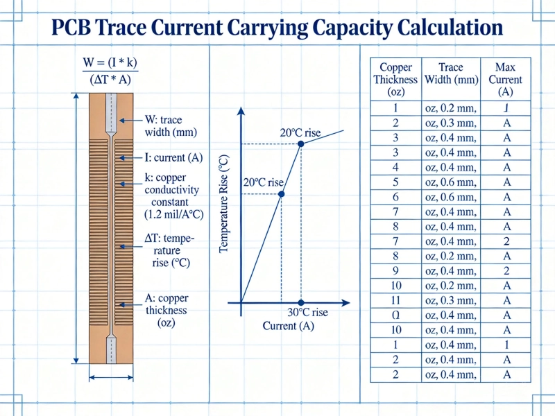
IPC-2152 Current Carrying Capacity: The Definitive PCB Trace Calculator GuideMay/21/2026
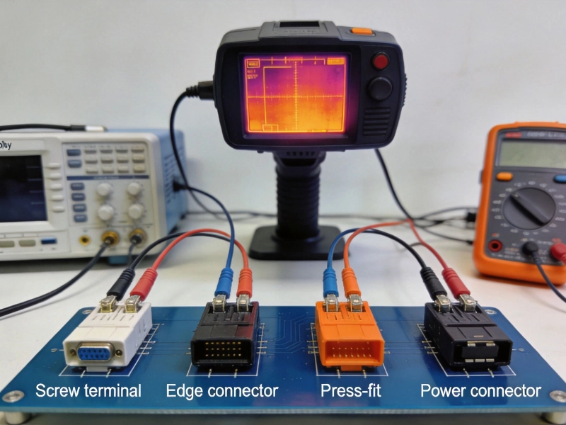
High Current PCB Connector Selection: Test Results and Real Performance DataMay/21/2026
High Current PCB Bus Bars vs. Heavy Copper Traces: Cost and PerformanceJuly/25/2026
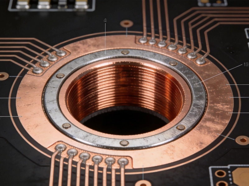
High Current PCB Annular Rings: Minimum Size vs. Reinforced SizeAugust/12/2026
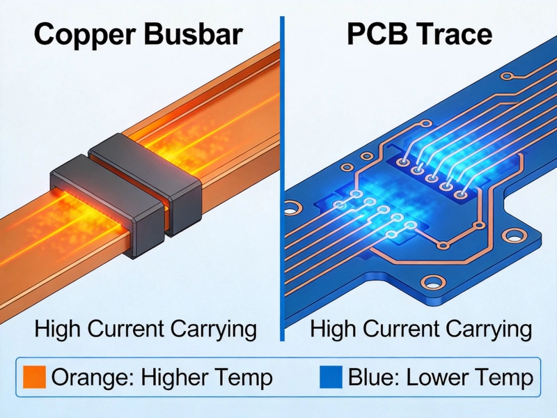
Bus Bar vs PCB Trace for High CurrentMay/21/2026
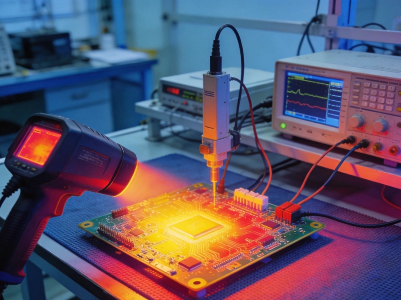
High Current PCB Testing: Thermal Imaging vs. 4-Wire Kelvin MeasurementJuly/22/2026
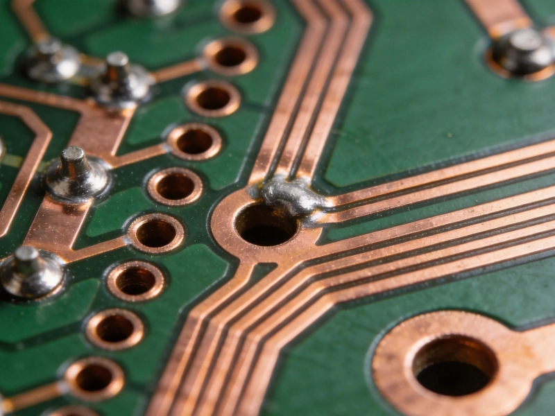
High Current PCB Solder Wicking: Tented Vias vs. Untented ViasSeptember/01/2026
High Current PCB vs. Standard PCB: A Real-World Thermal Stress TestJuly/09/2026