

When you're working with Heavy Copper PCBs that carry significant current, the silkscreen layer isn't just about component labels and logos anymore. You're dealing with high voltages, high currents, or both, and the spacing between different elements on your board suddenly becomes a safety-critical design consideration rather than a mere aesthetic or documentation feature.
High Current PCB design brings a whole set of clearance requirements that most standard PCB designers never have to think about. The rules that govern spacing between traces, pads, and other copper features under high voltage conditions are well-defined in industry standards, and ignoring them leads to field failures that are difficult to debug and potentially dangerous.
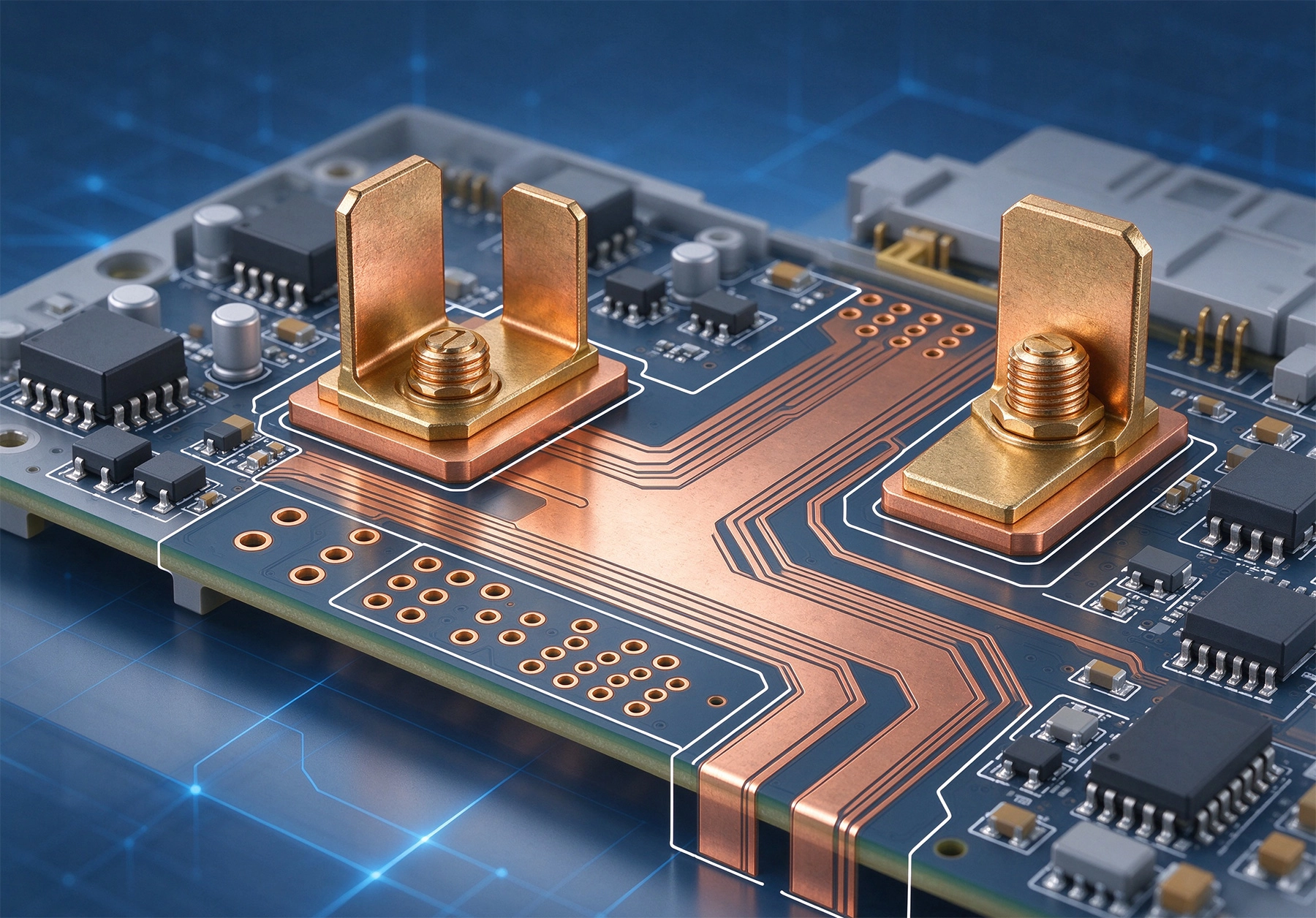
Before getting into specific numbers, it's worth being clear about the terminology. Clearance refers to the shortest straight-line distance through air between two conductive surfaces. Creepage is the shortest path along the surface of the insulating material between those same two points. For most PCB applications, creepage is longer than clearance because the surface path has to navigate around any slots, grooves, or other surface features.
Both measurements matter, but they respond differently to different threats. Clearance protects against arc-over through air under transient voltage conditions. Creepage protects against surface tracking under sustained contamination and moisture. When you're designing for High Current or high voltage, you need to consider both.
Several standards organizations have published requirements that inform PCB spacing decisions. Understanding which standard applies to your application determines a lot of your design constraints.
Ipc-2221 is the generic standard for Pcb Design and includes clearance tables based on voltage levels and environment. IPC-2221A provides additional guidance for high voltage applications specifically. These standards give you baseline requirements that work for most commercial applications.
The IPC clearance tables break down requirements by altitude (higher altitude means reduced air density and therefore reduced dielectric strength, requiring more clearance) and by coating condition (coated boards can use smaller clearances than bare boards because the coating adds protection against surface contamination).
If your product needs UL certification or CE marking, additional requirements apply. These safety standards are often more conservative than IPC recommendations because they're written with failure prevention as the primary goal rather than cost optimization.
For products that will be certified, it's worth getting the applicable standards early in the design process. Discovering spacing violations late in development when you're trying to get certification is an expensive problem to fix.
Different industries have different standards for their specific applications. Automotive Electronics follow AEC-Q standards that include spacing considerations. Medical devices have Iec 60601 requirements. Industrial equipment might follow IEC 61010. Make sure you're designing to the standard that actually applies to your end product, not just the most common one you know.
Here's where things get practical. The actual clearance numbers you need depend on the voltage difference between the elements in question and the environment your board will operate in.
For low voltage circuits, standard PCB spacing is usually adequate. Clearance of 0.1mm to 0.2mm works for most low voltage signal and Power Distribution applications. At these voltage levels, you're mostly concerned with preventing accidental shorts during assembly and avoiding leakage currents in humid environments rather than dielectric breakdown.
As you cross into medium voltage territory, spacing requirements increase noticeably. The IPC tables suggest roughly 0.5mm to 1.5mm clearance depending on altitude and coating. For a typical 120V or 240V AC application, you're looking at minimum clearances of around 1mm to 2mm for uncoated boards.
Heavy Copper boards handling this voltage range often have wide copper traces for Current Carrying Capacity. These traces can create Thermal Management challenges too—higher current means more heat, and that heat can affect the long-term reliability of spacing if the board runs hot.
Above 500V, spacing requirements become significant design constraints. Clearances of several millimeters might be necessary, and the layout of your board has to be planned around these constraints from the beginning. Simply shrinking traces and routing tighter won't help—you need the physical space between high voltage nodes.
At high voltage levels, you also start dealing with partial discharge effects. Small voids or imperfections in the dielectric material can lead to micro-arcs that slowly degrade the insulation over time. This is particularly relevant for heavy copper boards where the thicker copper layers might trap voids during lamination.
Heavy copper designs add complexity to clearance decisions beyond what standard boards face. The thicker copper means different manufacturing processes, different thermal behavior, and different reliability considerations.
With heavy copper, your traces are wider to carry the required current. This means adjacent traces or features are further apart naturally, which helps with clearance. But the wider traces also mean larger copper pads and components, which can complicate routing and reduce the available space for maintaining clearances elsewhere on the board.
The aspect ratio of Plated Through Holes also changes with heavy copper. Deeper plating to achieve the target Copper Thickness in vias can affect Annular Ring reliability. If you're routing high voltage near via structures, the plating thickness and barrel integrity become additional concerns.
High Current operation generates heat, and that heat affects the board's dielectric properties. Most PCB materials lose some dielectric strength at elevated temperatures. A clearance that's adequate when the board is at room temperature might be marginal when operating at full current in a warm environment.
Heavy copper designs need Thermal Analysis to ensure that operating temperatures stay within acceptable ranges. If your trace temperatures are running high, consider whether you need to increase clearances to compensate for the temperature-related reduction in dielectric strength.
The Surface Finish on your heavy copper traces affects their long-term reliability in high current or high voltage applications. Some finishes are more resistant to migration and dendrite growth than others. Enig (electroless nickel gold) is often preferred for high reliability applications, while Hasl (hot air solder level) finishes might present migration risks in certain high voltage scenarios.
Rather than trying to memorize tables, here's practical guidance for common scenarios you're likely to encounter in Heavy Copper Pcb design.
The clearance between your main power traces and ground or other low voltage nets depends on the voltage difference and the current involved. For most Power Electronics applications, maintaining at least 1mm clearance between primary power traces and any signal circuitry is a good starting point. Adjust up or down based on your specific voltage levels and the consequences of a failure.
If you have multiple power traces carrying high current, the spacing between them needs to account for both voltage isolation and thermal interaction. Two traces carrying high current generate heat that affects each other. Maintaining adequate spacing helps both with electrical isolation and Thermal Management.
Board mount connectors often have manufacturer-specified minimum spacing requirements. These specifications are based on the connector design and pin pitch, but you also need to consider the board-level clearance between connector pins and adjacent copper features. Heavy copper boards sometimes need slot cuts or other features to increase effective spacing near connectors.
The silkscreen layer on high current boards serves an important safety function beyond just component identification. Clear marking of hazardous voltage areas, current ratings, and safety warnings helps anyone working with the board understand the risks.
High voltage areas should be clearly marked with warning symbols and text. Standard hazard symbols help identify areas where special caution is needed. Many safety standards require specific wording for certification, so check your target standard for requirements.
Labeling your high current traces with their current ratings serves multiple purposes. It helps designers and technicians understand the board's capabilities, and it documents design intent that might not be obvious from the schematic. Some standards require this kind of marking for certified equipment.
Silkscreen keep-out markings help prevent assembly errors that could create safety hazards. Clearly marking areas where Component Placement is not allowed prevents someone from mounting a component too close to a high voltage trace or in a thermally problematic location.
Design rules for clearance need to account for manufacturing tolerances. The clearance you specify in your design files needs to survive the combined tolerances of your board fabrication, assembly, and any conformal coating or other post-assembly processing.
Copper etch tolerance, drill tolerance, and layer-to-layer registration all affect the actual clearance you'll get compared to your design intent. For tight clearance designs, working with your fab house to understand their actual capabilities is important. What looks good on your CAD screen might not match what comes off the production line.
Solder paste deposition, Component Placement, and reflow can all affect clearances. Tall components near high voltage areas are particularly concerning—they can reduce effective clearance by bridging the gap between high and low voltage areas. The physical height of placed components needs to be considered as part of your clearance analysis.
If your board will have conformal coating, potting, or other post-assembly processing, account for how that affects clearances. Conformal coating can reduce required clearances because it provides additional insulation. But if coating coverage is incomplete, you might end up with reduced effective clearance in some areas.
High Current PCB design needs to balance electrical safety with practical considerations like test access and serviceability. You need enough clearance to be safe, but not so much that the board becomes unwieldy or impossible to manufacture economically.
Test points should be placed where they can be accessed safely without risking accidental contact with high voltage nets. If your test access probe accidentally shorts across a high voltage gap, you might damage the board, the test equipment, or both.
Service documentation should clearly note any clearance requirements that service technicians need to be aware of. When a board comes back for repair, the technician needs to understand what spacing is critical and why.
Spacing violations in high current designs often come from treating the problem as purely electrical when it's really a systems engineering challenge. Here are the most common mistakes I see.
Designing clearances based only on nominal operating voltage, without accounting for transients and spikes. Power circuits generate switching transients that can far exceed the normal operating voltage. Your clearances need to handle the worst-case voltage the circuit will ever see, not just the steady-state voltage.
Ignoring altitude effects. Equipment that will operate at elevation experiences reduced air dielectric strength. A design that passes testing at sea level might fail at 3000 meters altitude. Know your operating environment and design for it.
Failing to consider contamination scenarios. Surface contamination from dust, flux residue, or fingerprints can dramatically reduce effective creepage. A clean board in a laboratory might perform fine, but the same board in a dusty factory might fail prematurely. Design for the contamination level your application will actually encounter.
Skipping Thermal Analysis. Clearance requirements at operating temperature are different from clearance requirements at room temperature. If your board runs hot, verify that your clearances are adequate at the actual operating temperature, not just at ambient conditions.
Once your board is designed, verification matters. Design rule checks in your CAD tool catch some spacing violations, but high current designs often need additional verification beyond basic DRC.
Hipot testing (high potential voltage testing) verifies that clearances can withstand the required test voltage without breakdown. The test voltage is typically higher than the maximum operating voltage by a safety factor specified in the applicable standard. Hipot testing catches manufacturing defects that might create weak spots in the isolation.
For very high voltage or high reliability applications, partial discharge testing might be appropriate. This sensitive test detects micro-arcs within the dielectric that would eventually lead to failure. Partial discharge testing is more expensive and time-consuming but provides confidence that your design will have long-term reliability.
Clearance requirements for high current heavy copper PCBs are not optional considerations—they're fundamental to safety and reliability. Understanding the applicable standards, accounting for manufacturing tolerances, and verifying through appropriate testing protects both your product and the people who will use it.
Start clearance planning early in your design process. Trying to add spacing after the layout is complete often means significant rework or a complete re-routing of critical signals.
Consider the complete environment your board will operate in, including temperature, altitude, contamination levels, and potential transient voltages. A conservative approach to clearance is almost always better than discovering spacing problems during certification testing.
Silkscreen markings serve an important safety function on high current boards. Clear warnings and ratings help prevent accidents during handling, testing, and service.
Contact us to discuss your High Current Pcb Design requirements and clearance specifications.
How Much Current Can a PCB Trace Carry? Complete Engineering GuideMay/20/2026
Best Material for High Current PCB Design: How to Choose the Right SubstrateJune/05/2026
High Current PCB Material Showdown: FR4 vs. Metal-Core vs. PolyimideJuly/14/2026
Best Material for High Current PCB DesignMay/21/2026
High Current PCB Solder Joints: Wave Soldering vs. Selective SolderingJuly/15/2026
High Current PCB EMI Shielding: Ground Pour vs. Shielding CansAugust/14/2026
High Current PCB Conformal Coating: Protecting Solder Joints Under Thermal StressAugust/06/2026
Why Your High-Power PCBs Overheat (And the 5 Methods That Actually Fix It)May/20/2026