

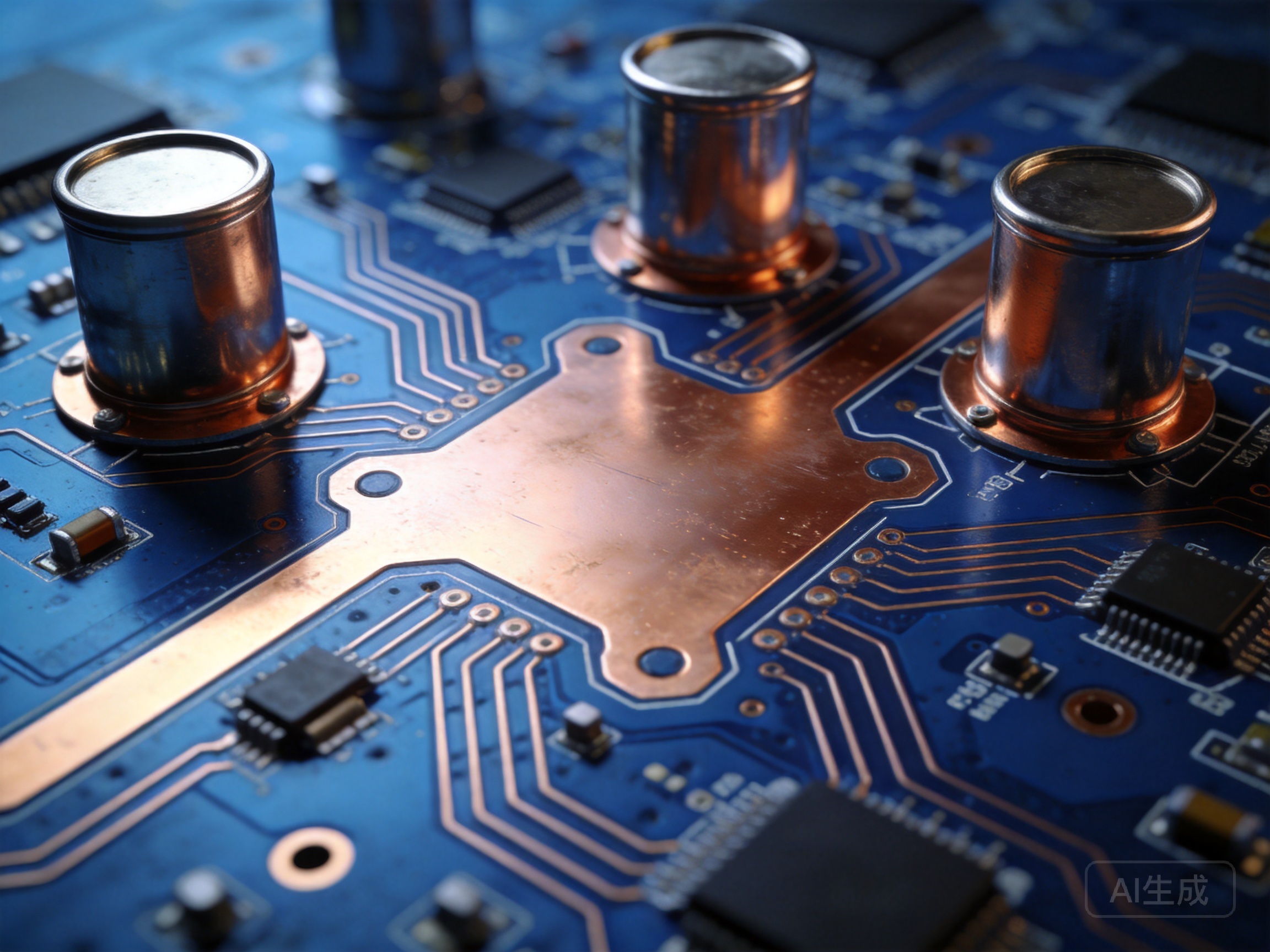
Electromagnetic Interference (EMI) represents one of the most critical design challenges in High Current PCB applications ranging from power supplies and motor drives to renewable energy inverters and Electric Vehicle systems. The high dV/dt and dI/dt rates inherent in switching Power Electronics generate significant electromagnetic emissions that can interfere with nearby sensitive circuitry, violate regulatory compliance standards, and even cause functional failures in the end product.
Two of the most commonly employed EMI mitigation techniques in High Current PCB design are ground pours and metallic shielding cans. Each approach offers distinct advantages and disadvantages, with different performance characteristics, implementation costs, and design trade-offs. Understanding the differences between these methods and their appropriate applications is essential for designing robust, compliant High Current electronic systems.
Before comparing shielding approaches, it's important to understand the specific EMI challenges presented by High Current PCBs. Switching power devices such as MOSFETs and IGBTs operate by rapidly switching high voltages and currents, creating sharp edges with harmonic components extending well into the gigahertz range. These high-frequency components radiate from circuit traces and components as electromagnetic energy, while also conducting through power and signal lines to other parts of the system.
High current designs face particular EMI challenges due to the larger loop areas often required for high-current carrying paths, which act as efficient antennas for radiating electromagnetic energy. Additionally, the high magnetic fields generated by large current flows can induce voltages in adjacent circuits, causing both conducted and radiated interference issues.
Regulatory standards such as FCC Part 15 in the United States and CISPR 22/EN 55022 in Europe establish strict limits on both conducted and radiated emissions from electronic equipment. Meeting these standards requires careful EMI mitigation throughout the design process, including appropriate shielding strategies.
Ground pouring, also known as copper flooding, involves filling unused PCB area with solid copper connected to the system ground. This technique provides multiple Emi Reduction benefits while also offering improved thermal performance and reduced impedance for ground connections.
Ground pours mitigate EMI through several complementary mechanisms. First, they provide a low-impedance return path for high-frequency currents, minimizing the area of current loops that act as radiating antennas. By providing a continuous ground plane adjacent to signal traces, ground pours also create controlled impedance transmission lines that reduce signal reflections and minimize unintentional radiation.
Additionally, ground pours act as a shield between traces on different layers of the PCB, reducing crosstalk between adjacent signals. The large copper area also provides effective electrostatic shielding, reducing capacitive coupling between circuit nodes and the external environment. For high current designs, ground pours also help distribute heat generated by power components, improving thermal performance and reliability.
To maximize Emi Reduction effectiveness, ground pours should be implemented following established design guidelines. In multilayer boards, dedicated ground planes provide the greatest benefit, but even two-layer designs can benefit significantly from properly designed ground pours on both layers connected with multiple vias.
Key design considerations include:
Ground pours offer several significant advantages for EMI mitigation in high current designs. They add no additional cost to the Pcb Manufacturing process beyond what's already required for the board itself, making them extremely cost-effective. They also improve thermal performance, reduce ground impedance, and simplify routing by eliminating the need for separate ground traces for each component.
However, ground pours have limitations as an Emi Shielding solution. They primarily provide shielding against electric fields and are much less effective against magnetic fields, particularly at lower frequencies where skin depth in copper is relatively large. Ground pours also cannot fully contain radiation from components mounted on the board surface, which can emit electromagnetic energy directly into the environment. Additionally, poor implementation with discontinuities and unoptimized return paths can actually increase EMI emissions in some cases.
Shielding cans, also known as RF shields or EMI shields, are enclosed metallic structures mounted over sensitive or noisy components to contain electromagnetic radiation. These cans are typically constructed from thin sheets of copper, tin-plated steel, or aluminum, and are soldered directly to the PCB ground plane around the perimeter of the area being shielded.
Shielding cans operate on the principle of Faraday cages, providing a complete conductive enclosure around the components or circuitry being protected. When electromagnetic radiation encounters the conductive shield, it induces electrical currents on the shield surface that are conducted to ground, preventing the energy from either escaping or entering the shielded enclosure.
Unlike ground pours, shielding cans provide effective attenuation of both electric and magnetic fields over a wide frequency range. The effectiveness of a shielding can depends on its conductivity, the thickness of the material, the size of any apertures in the shield, and the quality of the electrical connection between the shield and the PCB ground plane.
To achieve maximum EMI reduction, shielding cans must be carefully designed and implemented. The shield should form a complete enclosure around the protected circuitry, with minimal gaps or apertures. Any necessary openings for connectors, displays, or ventilation should be sized smaller than the shortest wavelength of concern, and may require additional shielding gaskets or honeycomb vent panels for high attenuation requirements.
The connection between the shielding can and the PCB ground plane is critical. The can should be soldered to a continuous ground ring around the shielded area, with multiple vias connecting this ring to the underlying ground plane to minimize connection inductance. For high-frequency applications, the spacing between these vias should be no more than 1/20th of the wavelength of the highest frequency being shielded.
Internal partitions within the shielding can can further reduce EMI by isolating different functional blocks within the shielded area, preventing interference between circuits sharing the same shield enclosure. Removable shielding can lids can provide access for rework and testing, though they may slightly reduce shielding effectiveness compared to permanently soldered enclosures.
Shielding cans offer several important benefits for EMI mitigation, particularly in high current designs. They provide significantly higher attenuation of both electric and magnetic fields compared to ground pours alone, often achieving 40-80 dB of attenuation across a wide frequency range. They can contain radiation from both Pcb Traces and mounted components, making them particularly effective for shielding noisy switching power circuits or sensitive RF circuitry.
Shielding cans also provide physical protection for components, reducing the risk of damage from mechanical impact or environmental contamination. They can also improve safety by providing a physical barrier between high-voltage circuitry and users.
However, shielding cans also have significant disadvantages. They add incremental cost to the product, both for the shield itself and for the additional assembly process required to install it. They increase the overall height and weight of the Pcb Assembly, which can be problematic in space-constrained applications. Shielding cans also complicate rework and testing, as they must be removed to access components underneath, potentially damaging the PCB or components in the process.
Additionally, shielding cans can create Thermal Management challenges by trapping heat generated by components within the shielded enclosure. This may require additional Thermal Management measures such as Thermal Vias, Heat Sinks, or vented shield designs that can compromise shielding effectiveness.
The choice between ground pours and shielding cans depends on multiple factors including EMI reduction requirements, cost constraints, space limitations, and thermal management needs. A side-by-side comparison across key performance dimensions can help inform design decisions.
Shielding cans provide significantly higher overall EMI attenuation, particularly for magnetic fields and higher frequency radiation. A well-designed shielding can provide 40 dB or more attenuation across a broad frequency range, compared to 10-20 dB of attenuation typically achieved through ground pouring alone. For designs needing to meet strict regulatory emission limits or containing very noisy circuitry, shielding cans may be the only viable option.
However, for many applications with moderate EMI requirements, well-implemented ground pours combined with good design practices (such as proper Component Placement, optimized routing, and filtering) may provide sufficient attenuation to meet regulatory requirements without the additional cost of shielding cans.
Ground pours offer essentially free EMI mitigation, requiring no additional components or assembly steps beyond what's already required for the PCB itself. In contrast, shielding cans add both material cost for the shield itself and labor cost for assembly. Custom shielding cans for complex shapes can be particularly expensive in low volumes, though standard off-the-shelf shield designs are available at lower cost.
It's important to consider total cost of ownership when making shielding decisions. While shielding cans add direct cost, they may reduce overall product cost by simplifying other aspects of the design, such as reducing filtering requirements or enabling higher component density that reduces overall board size.
Ground pours add minimal complexity to the Pcb Design process, though they require careful attention to return path management and via stitching to maximize effectiveness. They introduce no additional manufacturing complexity beyond standard PCB Fabrication processes.
Shielding cans require additional design effort to define the shield footprint, implement the ground ring and stitching vias, and ensure adequate clearance between the shield and components. They also add complexity to the manufacturing process, requiring an additional pick-and-place or hand soldering step to install the shield. Custom shield designs may also require additional tooling costs and longer lead times.
Ground pours significantly improve thermal performance by providing a large copper area for heat spreading from power components. In contrast, shielding cans can impede thermal performance by trapping heat within the shielded enclosure, unless specifically designed with thermal vents or integrated heat sink features.
For high current designs with significant Heat Dissipation requirements, ground pours offer clear thermal advantages, though careful shield design with integrated thermal management features can mitigate the thermal disadvantages of shielding cans.
Ground pours add no height or weight to the Pcb Assembly, making them ideal for space-constrained or weight-sensitive applications. Shielding cans add significant height, typically 2-10 mm or more depending on the components being shielded, and add weight to the assembly, which may be problematic for portable or aerospace applications.
Shielding cans do provide mechanical protection for components, which can be beneficial in applications subject to vibration, shock, or harsh environmental conditions.
In most high current designs, the optimal EMI mitigation strategy combines both ground pours and shielding cans, leveraging the advantages of each approach while minimizing their limitations. Several hybrid approaches have proven particularly effective.
A layered approach uses ground planes as the first line of defense against EMI, providing baseline attenuation and improved signal integrity, with selective use of shielding cans only for particularly noisy or sensitive circuit blocks. This approach minimizes cost while ensuring adequate EMI performance.
For example, in a typical motor drive design, the entire board would use extensive ground pouring and proper grounding techniques, with additional shielding cans only over the high-frequency switching power stage and sensitive control circuitry. This targeted approach provides the benefits of shielding only where needed, avoiding the cost of shielding the entire board.
To maximize the shielding effectiveness of ground planes, implement a solid ground plane on an inner layer adjacent to high-speed signal layers, with stitching vias connecting ground planes at regular intervals and around the board perimeter. This creates a faraday cage structure between layers, significantly reducing crosstalk and radiation between layers.
For high current designs, ensure that high-current return paths are isolated from sensitive analog or control circuitry, with separate ground regions connected at a single point to prevent noise coupling.
When using shielding cans, optimize their design for both performance and manufacturability. Use standardized shield footprints where possible to reduce cost and lead times. Include adequate clearance between the shield and components to accommodate manufacturing tolerances and prevent short circuits. Consider using two-piece shield designs with removable lids to simplify testing and rework.
For high-power applications, consider shields with integrated heat sink features or thermal apertures to improve Heat Dissipation, ensuring that any apertures are sized appropriately to maintain required shielding effectiveness. Use conductive gaskets between the shield lid and base to maintain shielding effectiveness for removable lid designs.
Even well-intentioned shielding implementations can fail to deliver expected performance due to common design errors. Avoid these pitfalls to maximize EMI mitigation effectiveness:
Ground Pour Mistakes:
Shielding Can Mistakes:
Both ground pours and shielding cans play important roles in EMI mitigation for High Current Pcb designs. Ground pours should be considered the foundation of any EMI mitigation strategy, providing cost-effective attenuation, improved thermal performance, and better signal integrity with no additional cost. For many applications with moderate EMI requirements, well-implemented ground pours combined with good layout practices may provide sufficient protection.
Shielding cans should be employed when additional attenuation is required beyond what ground pours alone can provide, particularly for designs with very noisy switching circuitry, sensitive RF components, or strict regulatory compliance requirements. When used selectively only for critical circuit blocks, shielding cans provide significant EMI reduction with minimal cost impact.
Most high-performance designs will benefit from a combination of both approaches, with ground planes providing baseline EMI reduction and shielding cans used selectively for particularly problematic circuits. By understanding the strengths and limitations of each method and applying them appropriately, designers can create robust, compliant high current electronic systems that meet EMI requirements while minimizing cost, size, and complexity.
High Current PCB Material Showdown: FR4 vs. Metal-Core vs. PolyimideJuly/14/2026
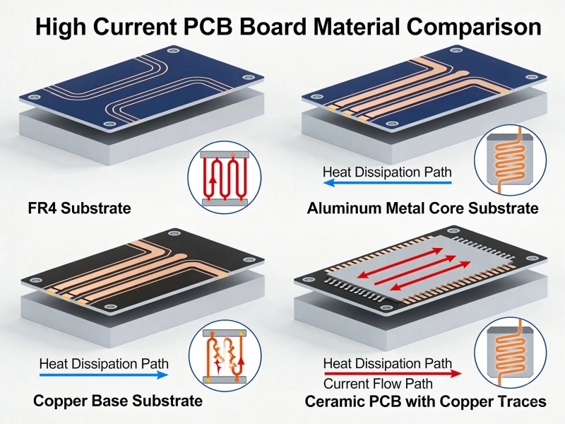
Best Material for High Current PCB Design: How to Choose the Right SubstrateJune/05/2026
High Current PCB Conformal Coating: Protecting Solder Joints Under Thermal StressAugust/06/2026
Best Material for High Current PCB DesignMay/21/2026
How Much Current Can a PCB Trace Carry? Complete Engineering GuideMay/20/2026
High Current PCB Solder Joints: Wave Soldering vs. Selective SolderingJuly/15/2026

High Current PCB Design for Railway Traction SystemsAugust/07/2026
High Current PCB Design for Renewable Energy MicrogridsSeptember/30/2026