

Every Power Electronics Design eventually runs into the same problem: a trace that carries 10 amps without complaint at room temperature becomes a reliability liability when the ambient climbs to 60°C or the board sits in a poorly ventilated enclosure. The culprit is almost never the Copper Weight itself — it's the connection between the component lead and the pad. Standard PCB pad plating is designed for Signal Integrity and solderability, not for surviving the thermal and mechanical stress that High Current imposes on a joint over thousands of hours.
If you've ever had a MOSFET or power resistor fail prematurely, watched a connector interface discolor from heat, or found a cracked solder joint on a high-current component, the pad design deserves a close look. This article breaks down the difference between reinforced plating and standard pads, walks through when the upgrade is worth it, and gives practical guidance on designing pad structures that hold up under real-world current loads.
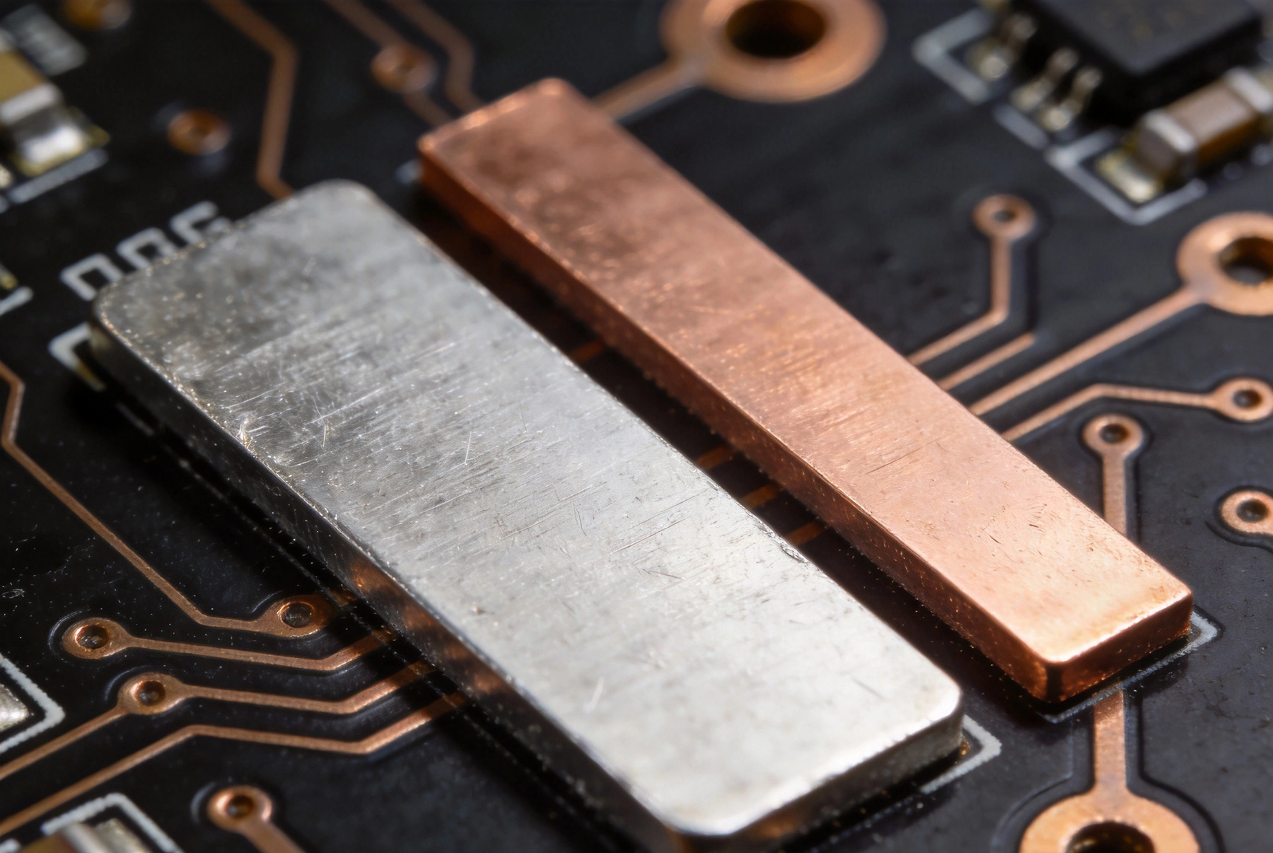
Standard PCB pads in most manufacturing processes use 1 oz or 2 oz copper, with plating thickness typically in the range of 0.5 to 1 mil (about 12–25 microns) of final finish. This is perfectly adequate for signal-level currents — a few hundred milliamps to a couple of amps. But when current climbs, the resistance of a thin pad creates significant I²R heating at the interface between the component lead and the pad surface.
That heat doesn't just warm the pad. It cycles the solder joint through expansion and contraction every time the load changes. Over hundreds or thousands of thermal cycles, the weakest point in the current path — which is usually the intermetallic layer between the lead and the solder — begins to degrade. The result is a gradual increase in contact resistance, more heat generation, and eventually an open joint or intermittent connection.
We see this pattern frequently in turnkey projects where engineers have correctly sized their power traces for current but left the pad design as a default from the schematic library. The trace carries the current fine; the pad is where the problem starts. Standard pad structures simply weren't designed for the sustained Current Density that power components demand.
Reinforced plating, sometimes called Heavy Copper plating, upz'd plating, or extended land plating, refers to increasing the thickness of the copper in the pad area and the finish plating (typically Enig, immersion tin, or hard gold) beyond standard production values. In practical terms, this means:
The mechanical effect is significant. A thick-plated pad has much lower resistance at the lead interface, generates less heat for the same current, and is more resistant to the Thermal Cycling that causes intermetallic fatigue. The solder joint is also larger and better anchored, which improves shock and vibration resistance.
Reinforced plating adds cost and usually requires a custom manufacturing step, so it's not something to apply everywhere. The decision should be driven by the current density at the pad and the operating environment. A few clear indicators that reinforced plating is worth the investment:
A practical design approach is to reserve reinforced plating for the specific pad areas that carry the highest current, while keeping the rest of the board on standard process. This targeted approach keeps tooling and manufacturing costs manageable while addressing the real failure points.
When specifying reinforced pad structures to your manufacturer, a few design parameters matter more than others. Getting these right the first time avoids the back-and-forth of re-quoting and re-tooling.
Plating thickness specification: State the minimum copper plating thickness in the pad area explicitly, in mils or microns. If you need 3 mil copper plating in the pad zone, say so — don't assume the manufacturer will interpret "Heavy Copper" the same way you do. Many manufacturers use different baseline thicknesses for standard vs. controlled-depth plating.
Pad geometry and keep-out zones: Reinforced plating often requires wider annular rings and larger pads to accommodate the plating process. Make sure your layout accounts for these clearance requirements early, especially if the board is dense. Trying to add reinforced pads to an already congested layout late in the design cycle often means redesigning adjacent routing.
Thermal relief strategy: Reinforced pads connected to large copper planes behave very differently thermally during soldering. The thermal mass of a heavily plated pad connected to a thick ground plane can make solder wetting sluggish, leading to cold joints if your reflow profile isn't adjusted. Thermal relief spokes (narrower connections between the pad and the plane) can help, but they reduce the current-carrying benefit. Working through this tradeoff with your assembly partner before the build is worth the time.
Via-in-pad for thermal and current management: Placing thermal or barrel vias directly in the pad under a power component is a common reinforcement technique. The via barrel effectively extends the current-carrying path through the board thickness, which dramatically improves Heat Dissipation away from the component body. For MOSFETs and power transistors, this is one of the most effective ways to manage junction temperature without adding a discrete heatsink.
Reinforced plating adds cost in several ways: the plating process itself is more expensive per panel, the tooling may need to be custom, and the tolerances are tighter so fewer boards pass the standard inspection criteria without extra verification. In our quoting data, reinforced plating on targeted pad areas typically adds 10–20% to the PCB Fabrication cost for the affected sections, with the total board cost increase depending on how much of the board area is affected.
On the assembly side, the main cost driver is solder paste volume. Thicker pads mean deeper stencil openings, which may require electroformed stencils instead of standard laser-cut stencils. Electroformed stencils are more expensive upfront but produce more consistent paste release for thick deposits.
Against those costs, consider what a field failure costs. A Power Electronics board returned from the field for a joint failure requires logistics, diagnosis, repair or replacement, and potentially reputation damage with your customer. For products where reliability is a selling point — industrial automation, medical power supplies, EV charging — the cost of reinforced plating is almost always justified for the high-current pad areas. For one-off prototypes or short-lifecycle consumer products, the math may not close, which is why volume and application context matter.
The Surface Finish on your pad matters as much as the copper plating thickness for long-term reliability. Standard finishes behave differently under high-current stress:
For most Power Electronics applications, we recommend ENIG with thicker-than-standard nickel or hard gold for the reinforced pad areas. The nickel thickness specification is the variable most often under-specified — make sure it's in your documentation and confirmed with your manufacturer before production.
Reinforced pads are one element of a broader current-carrying design strategy. They work best in combination with other techniques rather than in isolation.
Heavy copper traces: A reinforced pad connected to a standard 1 oz trace is a current bottleneck. The trace Copper Weight should match or exceed the pad capability. For 10+ amp traces, 3 oz to 6 oz copper is common; for extreme currents, some designs use 10 oz or heavier with routed channels to handle the thermal dissipation.
Bus Bar integration: For very high currents — above 50 A in many designs — the PCB alone can't carry the current economically. Copper bus bars soldered or bolted to reinforced PCB terminals provide the current path while the board handles the signal and control functions. This hybrid approach is standard in power inverters, EV battery management systems, and industrial UPS systems.
Thermal Management: Reinforced pads generate less heat than thin pads at the same current, but the heat they do generate still needs to go somewhere. Metal-backed substrates (IMS boards), Thermal Vias, and direct chassis mounting of power components all help keep the joint temperature within safe limits. Designing the thermal path alongside the current path is more effective than treating them as separate problems.
A few patterns show up repeatedly in designs that end up with pad-related field failures:
Using standard library pads for power components. This is the most common mistake. A MOSFET with an RDSon of 2 milliohms carrying 20 A generates 0.8 W at the device — most of which flows through the drain pad. Standard pad structures simply weren't sized for this. Always verify pad dimensions and plating against the component datasheet's current rating, not just the datasheet footprint.
Ignoring the derating curve for pad current capacity. PCB pad current capacity charts in standards like Ipc-2152 are derived for continuous DC current under specific board conditions. Real-world loads — pulsed currents, AC currents with high peaks, uneven duty cycles — stress the joint differently. When in doubt, build in margin. Designing for 150% of the expected peak current is a reasonable engineering practice.
Plating thickness specified in the fab notes but not verified in the fabrication. If the plating thickness matters for your design, verify it with your manufacturer explicitly. Ask for cross-section reports on the first article. Assumptions about "standard heavy copper" can lead to boards that arrive with 1 oz copper where you needed 3 oz.
There is no single answer because it depends on pad size, copper weight, thermal relief configuration, ambient temperature, and acceptable temperature rise. As a rough starting point, a standard 1 oz copper pad of typical SMD dimensions (say, 1206 or SOIC scale) can carry 2–3 A continuously before generating significant heat at the joint. Above 5 A on a standard pad, most engineers start considering reinforcement. For designs where thermal cycling or vibration is a factor, the threshold is lower — reinforced plating is often justified at 3 A or above in those conditions.
Yes, and this is the most common approach. The manufacturer can define the reinforced pad areas in the tooling and apply heavy plating selectively. This keeps the bulk of the board on standard process while addressing the specific high-current pad locations. Selective reinforcement adds cost compared to uniform heavy copper but is far cheaper than building the entire board to heavy copper specifications.
Reinforced copper pads with appropriate surface finishes (ENIG, hard gold, immersion tin) solder normally with standard profiles. The main solderability risk is if the pad surface is contaminated or if the nickel layer in ENIG is too thin, causing the gold to diffuse into the copper and creating a poor wetting surface. With proper specification and QA, solderability is not an issue. Thicker pads do require attention to paste volume and potentially a slightly higher peak reflow temperature to ensure full fillet formation, which your assembly partner should account for in the profile setup.
Reinforced plating typically refers to thicker copper in specific pad and trace areas on an otherwise standard board. Heavy Copper Pcb (sometimes called power copper or upz'd copper) refers to the entire board being built on thicker copper — often 3 oz, 6 oz, or heavier across all traces and planes. Heavy copper boards are structurally different from standard boards and require different lamination and plating processes. Reinforced plating is a more surgical approach: you get thicker copper exactly where you need it, without the cost and lead time implications of a full heavy copper build.
Request a cross-section analysis on the first article from each new panel. The lab will pot a sample of the board, cut it at the pad location, polish it, and measure the copper and finish plating thickness under a microscope. This is the definitive verification. For production boards, your manufacturer should be performing coupon testing on each panel as part of their standard IPC process. Ask to see the coupon data for the plating thickness on the job traveler.
A Deep Dive into High Current PCB Design for Solar InvertersJuly/17/2026
Designing a High Current PCB Motor Driver: Avoiding EMI PitfallsJuly/14/2026
Why Your High-Power PCBs Overheat (And the 5 Methods That Actually Fix It)May/20/2026
High Current PCB Design for Aerospace Power DistributionSeptember/08/2026
High Current PCB Design for Telecommunications Base StationsSeptember/18/2026

High Current PCB Design for Medical Imaging EquipmentSeptember/10/2026
IPC-2152 Current Carrying Capacity Calculation GuideJune/03/2026
High Current PCB Design for Electric Boat PropulsionOctober/26/2026