

Designing printed circuit boards for High Current applications demands precision in trace width calculations. The copper conductors that carry power through your PCB must dissipate heat while maintaining structural integrity and avoiding voltage drop problems. Engineers face a fundamental choice: follow the standardized Ipc-2152 approach with dedicated calculators, or rely on the simpler empirical formulas that have guided Pcb Design for decades.
This choice carries real consequences. Undersized traces overheat and fail catastrophically. Oversized traces waste valuable board space and increase material costs. Understanding both approaches—and their relative strengths—enables you to make informed decisions for your specific application requirements.
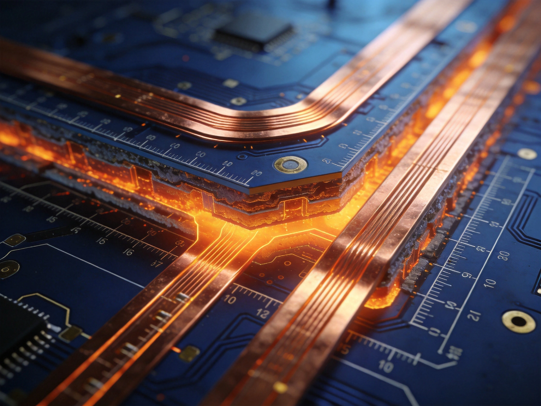
Before Ipc-2152, engineers relied primarily on charts and formulas derived from empirical testing conducted in the 1950s and 1960s. These original guidelines appeared in Ipc-2221, the generic standard for Pcb Design, and featured charts correlating trace width, thickness, and current-carrying capacity with allowable temperature rise. While practical for their time, these charts suffered from significant limitations that became increasingly problematic as electronics miniaturization progressed.
The original charts assumed external traces in free air—a condition rarely matching actual PCB deployment environments. They also failed to account adequately for trace thickness variations, copper foil roughness effects, and the thermal properties of the PCB substrate. Designers working on high-density boards with internal traces often found the charts provided unreliable guidance.
Recognizing these shortcomings, IPC undertook comprehensive research to develop a more accurate and versatile standard. Published in 2009 and subsequently updated, IPC-2152: "Standard for Determining Current Carrying Capacity in Printed Board Design" represents the most rigorous investigation into PCB Current Carrying Capacity to date. The standard incorporates extensive experimental data, thermal modeling, and consideration of multiple variables affecting trace performance.
The research behind IPC-2152 examined traces under various conditions: internal vs. external, with and without thermal relief, different board orientations, and natural vs. forced convection environments. This breadth of testing provides designers with a scientifically grounded foundation for their calculations—a significant improvement over the limited data underlying earlier guidelines.
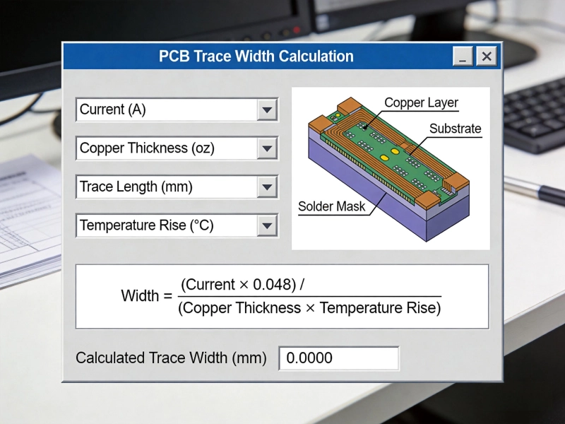
IPC-2152 calculators require several key parameters to produce trace width recommendations. These include the desired current carrying capacity in amperes, the acceptable temperature rise above ambient, trace length, whether the trace runs on external or internal layers, and the Copper Weight or thickness. Some advanced calculators also incorporate trace spacing, board orientation, and the presence of adjacent heat-generating components.
The temperature rise parameter deserves particular attention. A 10°C rise may be acceptable for a power supply operating in a controlled environment, while the same rise might push components beyond ratings in a densely packaged consumer device. Defining an appropriate temperature rise requires understanding both your thermal environment and the temperature sensitivity of nearby components.
IPC-2152 calculators typically output the minimum trace width required to safely carry the specified current without exceeding the target temperature rise. More sophisticated tools provide additional outputs including voltage drop calculations, power dissipation estimates, and Thermal Resistance values. Some also generate graphs showing the relationship between trace width and temperature rise across a range of currents.
It's important to note that IPC-2152 calculators generally provide conservative results—deliberately erring on the side of safety. This conservatism reflects the standard's development process, which tested boards under worst-case conditions. Your specific application may permit narrower traces if thermal testing validates acceptable performance.
The most widely used empirical formula for Trace Width Calculation originated from observing the relationship between trace cross-sectional area and current capacity. The fundamental equation takes the form of Area = (Current / k)^(1/0.725), where k is a constant derived from empirical testing. Different values of k produce formulas optimized for internal vs. external traces or specific temperature rises.
A commonly cited formula for external traces uses k = 0.048, yielding:
Width (mils) = (Current / (0.048 × Temperature Rise^0.44))^(1/0.725)
For internal traces, the formula adjusts with k = 0.024, reflecting the reduced Heat Dissipation of traces embedded within the PCB stack-up. These formulas produce reasonable estimates for many applications but represent simplifications of the actual thermal and electrical physics involved.
Empirical formulas offer immediate accessibility—engineers can implement them in spreadsheets or design scripts without specialized software. The simplicity enables quick iterations during schematic design before finalizing PCB layouts. For projects without access to IPC-2152 calculators or where order-of-magnitude estimates suffice, empirical formulas provide useful starting points.
These formulas also benefit from decades of field validation. Countless successful PCB designs have relied on empirical calculations, suggesting adequate accuracy for many practical applications. When design margins are generous and environmental conditions are benign, empirical formulas often produce perfectly adequate results.
Empirical formulas derive from limited experimental datasets that may not adequately represent modern PCB materials and constructions. Changes in laminate chemistry, copper foil treatments, and manufacturing processes can invalidate assumptions underlying these formulas. The formulas also struggle to account for the complex thermal interactions present in multi-layer boards with power and ground planes.
Most empirical formulas assume a specific Copper Thickness—typically 1 oz/ft²—without providing reliable adjustment factors for thicker or thinner foils. This limitation becomes increasingly problematic as designs push toward either ultra-thin high-density traces or Heavy Copper Power Distribution networks.
The most significant differences between IPC-2152 and empirical methods appear in internal trace calculations. Empirical formulas typically apply a blanket 50% reduction factor for internal traces compared to external traces. IPC-2152, however, provides more nuanced guidance reflecting the actual thermal environment of internal layers.
Research underlying IPC-2152 shows that the internal vs. external ratio varies with trace width and board construction. For narrow traces on internal layers, the derating factor may be closer to 35%, while wide traces approaching power plane boundaries might see only 20% reduction. These refinements matter significantly for high-current Bus Bar Design where trace widths of several millimeters are common.
Both calculation methods respond to temperature rise targets, but with different sensitivities. Empirical formulas typically assume a fixed temperature rise and provide trace widths for those conditions. IPC-2152 calculators often reveal non-linear relationships between temperature rise and required trace width that empirical formulas obscure.
For high-current applications, this non-linearity matters. Doubling the acceptable temperature rise from 10°C to 20°C does not halve the required trace width as simple scaling would suggest. IPC-2152 captures this behavior accurately, while empirical formulas may produce either overly conservative or dangerously optimistic results depending on the specific conditions.
IPC-2152 calculators are essential for applications where accuracy directly impacts safety, reliability, or cost. Power Electronics, automotive systems, and industrial controls—all domains where PCB failures can have serious consequences—benefit from the standard's rigorous methodology. Any design where trace width optimization could reduce material costs significantly also justifies using IPC-2152, as the investment in accurate calculation pays returns through right-sized traces.
Multi-layer boards with internal high-current traces represent another clear application. The thermal environment of internal layers differs substantially from external conditions, and IPC-2152 provides much better guidance than empirical rules of thumb. Similarly, designs incorporating Thermal Relief Patterns, Heavy Copper layers, or special Thermal Management techniques are best evaluated using the standard's comprehensive framework.
For prototyping, proof-of-concept work, and low-power applications, empirical formulas often provide adequate guidance without requiring specialized tools or extensive parameter specification. Hobbyist projects, academic work, and early-stage development where design margins are deliberately generous can proceed effectively with simpler calculations.
Empirical formulas also serve well for quick feasibility assessments. Before investing time in detailed IPC-2152 analysis, engineers can use simplified calculations to determine whether a design approach is viable. If empirical formulas indicate traces would need to be wider than the board permits, there's no need for sophisticated analysis—the fundamental approach requires revision.
High Current PCB design frequently incorporates Thermal Management techniques beyond simple trace widening. Thermal Vias connecting surface traces to internal planes dramatically improve Heat Dissipation, effectively increasing current capacity without consuming additional board width. IPC-2152 calculators can accommodate thermal via effects, but accurate modeling requires understanding via Thermal Resistance and current sharing between the trace and underlying planes.
For extremely High Current applications, adding external copper pours connected through Thermal Vias to internal planes creates effective Bus Bar structures. These composite conductors combine the favorable Current Distribution of planes with the accessibility of surface routing for component termination.
High current traces sometimes employ slotting—creating narrow gaps in ground planes adjacent to power traces to concentrate current in dedicated conductors rather than spreading across plane copper. This technique requires careful analysis, as slotting can create unintended impedance discontinuities or electromagnetic interference issues in adjacent signal traces.
Windowed planes, where plane copper is selectively removed around high-current routes, provide another thermal management approach. These windows allow heat to escape from internal traces while maintaining plane continuity in other areas. The trade-off involves routing flexibility and potential plane Current Crowding effects at window boundaries.
Regardless of calculation method, empirical validation remains the ultimate verification for High Current PCB design. Thermocouple measurements during prototype testing provide direct confirmation that traces operate within acceptable temperature limits. Infrared thermal imaging offers non-contact mapping of temperature distribution across the board, revealing hot spots that calculations might miss.
Long-term reliability testing under representative environmental conditions catches issues that short-term measurements might not reveal. Thermal Cycling, humidity exposure, and extended operation at rated current identify failure modes including trace delamination, pad lifting, and solder joint degradation that can emerge over time despite adequate initial calculations.
Choosing between IPC-2152 calculators and empirical formulas for high current Pcb Trace Width design requires matching the calculation method to the application's requirements. IPC-2152 provides superior accuracy through rigorously validated data and comprehensive modeling of thermal effects. For safety-critical applications, high-current Power Distribution, or cost-sensitive designs requiring trace optimization, the standard's investment in accuracy pays dividends.
Empirical formulas retain their utility for rapid prototyping, educational applications, and designs with generous margins. Their simplicity enables quick iterations and reasonable estimates without specialized tools. Understanding both approaches—and their respective limitations—equips engineers to select the right method for each project's unique constraints.
The most robust design practice combines calculation with validation. Use IPC-2152 calculators for definitive trace sizing, then verify through thermal testing. This combination of rigorous analysis and empirical confirmation ensures designs that perform reliably throughout their operational life.
High Current PCB Component Placement: Grouping vs. Distributed LayoutJuly/21/2026
High Current PCB Edge Connectors: Current Rating and Thermal LimitsSeptember/20/2026
High Current PCB Pad Design: Reinforced Plating vs. Standard PadsJuly/28/2026
High Current PCB Conformal Coating: Protecting Solder Joints Under Thermal StressAugust/06/2026
High Current PCB Embedded Copper: Internal vs. External Heat DissipationSeptember/26/2026
High Current PCB EMI Shielding: Ground Pour vs. Shielding CansAugust/14/2026
High Current PCB Trace Width Calculator: Complete Guide with Formulas and ExamplesMay/20/2026
High Current PCB Via Plating: 1mil vs. 2mil Thickness Reliability TestAugust/03/2026