

Industrial welding equipment pushes the boundaries of what a printed circuit board is expected to do. Unlike consumer electronics, where currents are measured in milliamps and thermal margins are generous, welding machines demand PCB designs that carry tens to hundreds of amps without overheating, delaminating, or failing prematurely. The stakes are high — both in terms of equipment cost and operator safety.
Designing a PCB for industrial welding is a discipline that sits at the intersection of Power Electronics, thermal engineering, and mechanical ruggedness. This article walks through the core considerations, trade-offs, and design practices that distinguish a successful high-current welding PCB from one that will fail in the field.
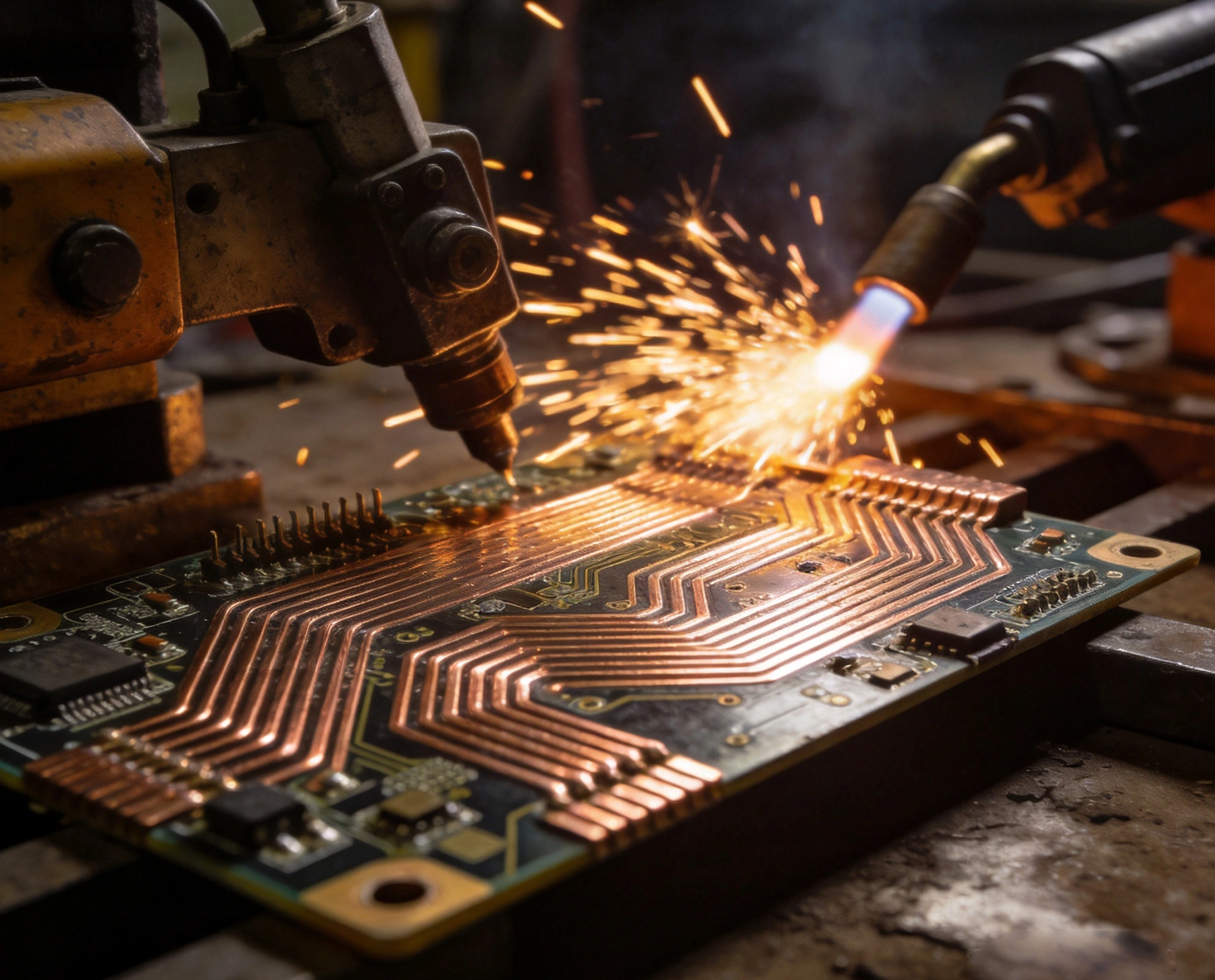
Welding machines — whether based on MIG, TIG, stick, or plasma arc processes — share a common electrical characteristic: they require large, controlled currents to generate the arc that melts and fuses metals. A typical industrial MIG welder might operate at 150 to 300 amps, while heavy-duty submerged arc systems can exceed 1,000 amps.
The PCB in such a system rarely carries the full welding current directly — that is typically handled by bus bars and heavy cables. Instead, the PCB manages the control, sensing, and power switching functions: MOSFET or IGBT gate drives, current feedback from shunt resistors or Hall effect sensors, PWM control logic, and operator interface circuits. Even at these lower current levels — tens of amps in the switching path — conventional Pcb Design assumptions break down.
The single most important decision in a high-current Pcb Design is Copper Weight. Standard PCB Fabrication uses 1 oz/ft² (35 µm) copper, which is adequate for signal traces but wholly insufficient for any trace carrying more than a few amps of continuous current.
For welding equipment PCBs, copper weights of 2 oz/ft² (70 µm), 3 oz/ft² (105 µm), or heavier are standard. Some designs for extreme current densities use 6 oz/ft² (210 µm) or more. The relationship between copper cross-section and current capacity is not linear — doubling Copper Thickness more than doubles the current-carrying capacity because thermal dissipation improves as well.
When specifying Copper Weight, confirm with your manufacturer that they can reliably plate uniform copper in the required thickness, particularly in slots, via barrels, and around plated through-holes. Inconsistent copper distribution is one of the most common causes of unexpected failures in Heavy Copper boards.
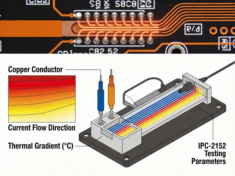
Ipc-2152, the standard for determining current-carrying capacity in PCBs, provides charts and formulas for sizing traces based on copper weight, temperature rise, and ambient conditions. For high-current welding applications, the key takeaway is that temperature rise must be kept conservative — typically 10°C to 20°C above ambient — which drives significantly wider traces than a casual calculation might suggest.
As a rough reference, a 1 oz/ft² trace carrying 10 amps at a 10°C rise needs approximately 100 mils (2.5 mm) of width. Scale that to 50 amps, and the same copper weight requires traces over 500 mils wide — which is often impractical. This is why Heavy Copper boards with 3 oz or 6 oz copper are essential for these applications.
Modern PCB design software can model Trace Current Capacity using Ipc-2152 calculators, but these tools should be validated against thermal simulation or empirical testing for designs where failure has serious consequences.
Traces on the outer layers of a PCB benefit from convective cooling by ambient air and have approximately twice the current capacity of identical internal traces. Where possible, route high-current paths on the outer layers and maximize exposure to airflow. In forced-air or liquid-cooled welding equipment, external trace cooling is even more effective.
High Current always means heat. In a welding PCB, Thermal Management is not an afterthought — it is a primary design driver. Key strategies include:
Connect high-current pads to internal Power Planes using arrays of Thermal Vias. These vias provide a low-thermal-resistance path to inner copper layers, which act as Heat Sinks. Thermal relief spokes — small gaps around a pad that reduce heat loss during soldering while still providing a conductive path — should be used thoughtfully: too many spokes and the Thermal Resistance increases; too few and solderability suffers.
Rather than routing high-current traces as narrow lines, use filled polygon pours or dedicated power plane layers for the main current paths. Planes distribute current more evenly and dissipate heat across a larger area. In a 4-layer or 6-layer board, allocating one or two full inner layers as Power Planes is a standard and effective approach.
Power semiconductors — IGBTs, MOSFETs, diodes — are the dominant heat sources on a welding PCB. Place them for maximum airflow access, orient them to take advantage of natural convection channels, and separate them thermally from temperature-sensitive control circuitry. In tight enclosures, active cooling — fans or liquid cold plates — may be necessary to keep junction temperatures within safe limits.
Industrial welding equipment operates in harsh conditions: high ambient temperatures, vibration, dust, and moisture. Standard FR-4 substrate (Tg around 130–140°C) may be adequate for the control electronics housed in a climate-controlled cabinet but is insufficient for boards mounted near the welding arc or in unshielded enclosures.
High-Tg FR-4 (Tg 150–170°C or higher) provides a larger thermal margin before the substrate begins to soften. For the most demanding applications, polyimide (Kapton-based) laminates offer superior thermal and mechanical performance, though at significantly higher cost.
When specifying materials, also consider the glass transition temperature relative to the maximum operating temperature the board will experience, including transient thermal spikes during welding operations. A board that regularly approaches its Tg will experience progressive delamination over time, even if no immediate failure occurs.
Vias present a paradox in High-current Pcb design: they are necessary for connecting layers, but a standard plated-through via barrel carries limited current before overheating. For welding equipment, two strategies address this:
The current rating of a via depends on its diameter, plating thickness, and thermal connection to copper planes. Rule-of-thumb estimates suggest a 0.5 mm diameter via with standard 1 oz plating carries roughly 1 amp safely. At 50 amps, you need dozens of parallel vias or a much larger barrel.
A welding machine is a rugged piece of equipment, and its PCBs must survive more than thermal stress. Vibration and mechanical shock are constant companions in industrial environments. Key design practices include:
Welding equipment operates at high voltages — 240V, 480V, or three-phase inputs are common — and the control PCB must interface safely with these potentials. Creepage And Clearance distances between high-voltage and low-voltage circuits are mandated by safety standards such as IEC 60950-1 (now IEC 62368-1 for audio/video and IT equipment) and Iec 60601-1 for medical-grade equipment.
Key isolation requirements include:
Failing to meet Creepage And Clearance requirements is not just a compliance issue — it creates a direct safety hazard for operators and end-users. Engage with a certified safety engineer or use recognized design-for-safety checklists before finalizing a welding Pcb Layout.
High-current PCBs push the limits of standard fabrication capabilities. Before releasing your design for manufacture, confirm the following with your PCB vendor:
A close working relationship with your fabrication partner early in the design process prevents costly surprises during production. Share your thermal and current requirements upfront and ask for their recommended stackup and material configuration.
No high-current welding PCB should go to production without thorough validation testing:
What copper weight do I need for a 100-amp trace on a welding PCB?
With a conservative 10°C temperature rise target and outer layer routing, a 3 oz/ft² copper weight requires approximately 400–500 mils (10–12 mm) of trace width. Using an inner layer halves the effective width due to reduced cooling. For such high currents, a dedicated power plane is far more practical than a single trace.
Can I use standard FR-4 for a welding machine PCB?
It depends on placement. Boards in climate-controlled enclosures using FR-4 (preferably high-Tg) are generally acceptable. Boards mounted near heat sources or in uncooled enclosures in hot factory environments should use high-Tg FR-4 or polyimide for adequate thermal margin.
How do I calculate Via Current Capacity for parallel via arrays?
A conservative estimate for a standard 0.4 mm diameter plated via is 0.5–1.0 amp per via. At 30 amps, you need 30–60 parallel vias minimum. Increase the count further if thermal relief to planes is suboptimal or if the board operates at elevated ambient temperatures.
What is the most common failure mode in high-current welding PCBs?
Trace overheating and delamination are the most frequent field failures. Traces that run too narrow for their current load generate localized hotspots that accelerate copper migration, void formation in plated holes, and eventually opens or shorts. Delamination follows when the substrate repeatedly exceeds its glass transition temperature.
Do I need conformal coating on a welding PCB?
If the equipment operates in dusty, humid, or corrosive environments — common in fabrication shops — conformal coating significantly extends board life. Choose an acrylic or urethane coating rated for the operating temperature range and re-coatability requirements.
IPC-2152 Current Carrying Capacity Calculation GuideJune/03/2026
High Current PCB Design for Aerospace Power DistributionSeptember/08/2026
High Current PCB Design for Audio Amplifiers: Avoiding Ground LoopsSeptember/14/2026
High Current PCB Design for High-Voltage DC TransmissionSeptember/24/2026
High Current PCB Design for High-Frequency Switching RegulatorsSeptember/04/2026
Plated Through Hole Current Rating: Complete Guide for PCB DesignersMay/21/2026

High Current PCB Thermal Relief: Full Connect vs. Modified SpokesJuly/16/2026
High Current PCB Design for Telecommunications Base StationsSeptember/18/2026