

Designing high-current PCBs presents challenges that go far beyond standard digital electronics. When your board must handle tens or hundreds of amperes, every placement decision impacts thermal performance, electromagnetic interference, and system reliability. One of the most fundamental choices engineers face is whether to group high-power components together or distribute them across the board.
Neither approach is universally better—the optimal strategy depends on your application's specific requirements. Understanding the tradeoffs between grouping and distributed layouts enables you to make informed decisions that optimize performance, manufacturability, and cost.
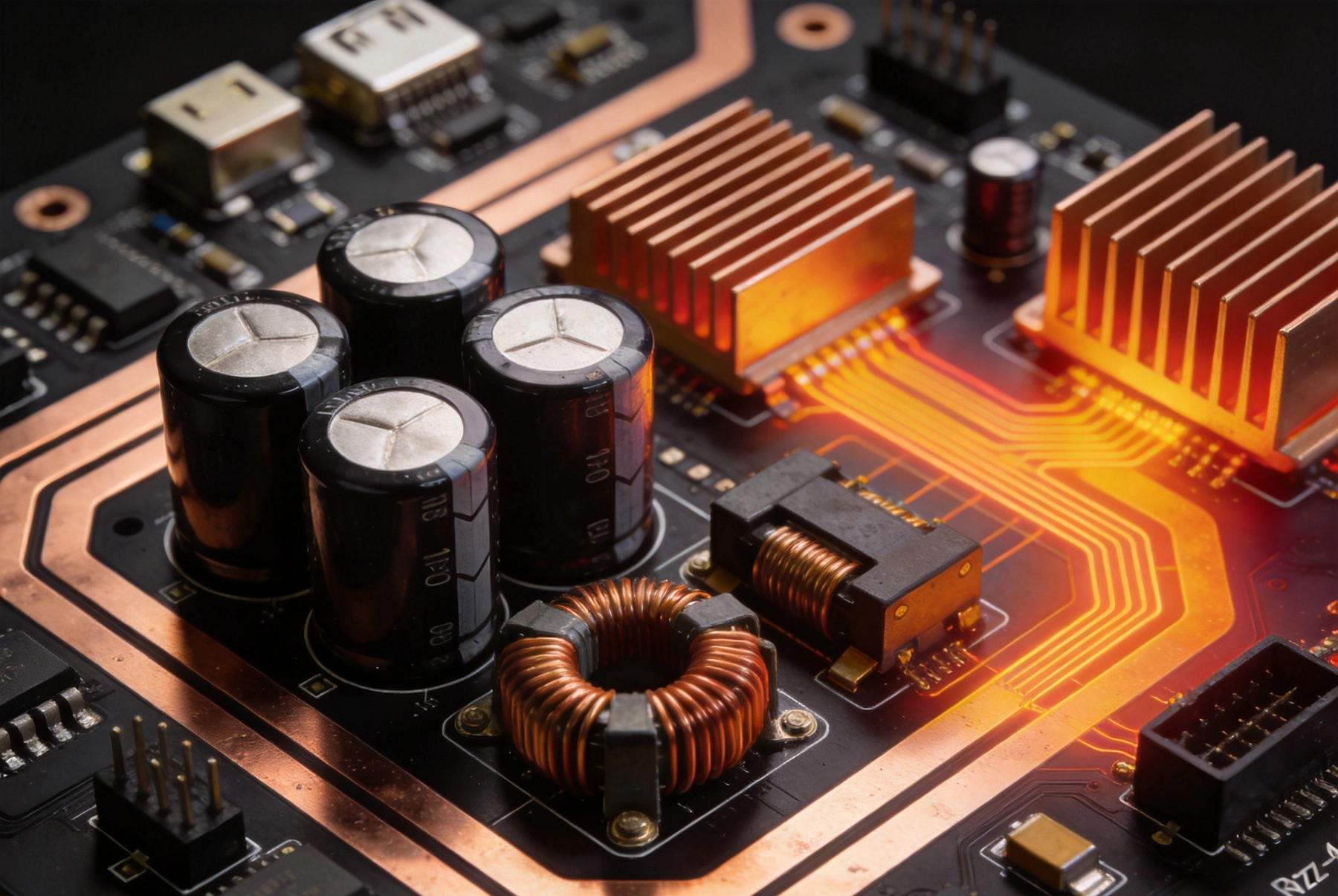
Before evaluating placement strategies, it's essential to understand what makes high-current design different from conventional Pcb Layout.
Standard Pcb Traces designed for digital signals typically carry milliamperes. High-current applications demand traces that can handle 10A, 50A, or even 100A+. This requires:
These requirements fundamentally change layout constraints. High-current paths need physical space, and component placement must accommodate these oversized conductors.
Current flow generates heat. At high currents, even small resistances create significant power dissipation. A 10mΩ trace carrying 50A dissipates 25W—enough to overheat a small board area rapidly. Component placement directly affects Thermal Management because:
In high-current applications, parasitic effects that are negligible in digital circuits become significant. Trace inductance causes voltage spikes during switching transients. Resistance creates voltage drops that affect regulation accuracy. Component placement directly influences these parasitics:
A grouped layout concentrates high-current components in one section of the PCB, typically near the power input connector or the primary power stage.
Minimized Parasitic Inductance: By placing power components close together, you minimize the length of high-current paths. Shorter traces mean lower inductance, which reduces voltage spikes during switching and improves power supply response time. For switching regulators operating at high frequencies, this advantage is critical.
Efficient Current Path: Grouping enables a logical flow from input to output without long detours across the board. Current can flow directly from input connector through protection devices, switching elements, and magnetics to the output. This straightforward routing reduces voltage drop and improves efficiency.
Simplified Thermal Sink Design: When heat-generating components are grouped, you can design a concentrated Thermal Management solution. A single heatsink, Thermal Pad, or metal-core substrate section can serve multiple components. This simplification often reduces assembly complexity and cost.
Emi Containment: High-current switching generates electromagnetic interference. Grouping power components confines Emi sources to one board section, making shielding and filtering more manageable. You can implement localized EMI countermeasures without affecting the entire board design.
Manufacturing Simplicity: Grouped layouts often simplify assembly processes. Heavy components like large inductors and transformers can be placed in one area, reducing handling complexity. High-voltage clearance requirements are easier to satisfy when confined to a single section.
Thermal Concentration: The most significant disadvantage is heat concentration. When multiple high-power components are placed together, their thermal contributions combine. Local temperature can rise dramatically, potentially exceeding component specifications or affecting nearby sensitive circuits.
Board Real Estate Competition: Grouping power components may require dedicating a substantial board section to power circuitry. This reduces available space for signal routing and other functions, potentially forcing compromises elsewhere in the design.
Heat Sensitive Component Risk: Temperature-sensitive components near the power section may experience thermal stress. Careful placement and thermal barriers are essential to prevent heat migration into sensitive areas.
Copper Weight Requirements: Concentrated high-current paths may require extremely Heavy Copper in one board section while the rest of the board uses standard weights. This mixed copper requirement can increase Manufacturing Cost and complexity.
A distributed layout spreads high-current components across the PCB, positioning them near their loads or in locations that optimize individual thermal and electrical requirements.
Thermal Distribution: By spacing heat-generating components across the board, you prevent local hotspots. Heat spreads more evenly, reducing peak temperatures and improving overall thermal performance. This approach is essential when board-level cooling is limited.
Proximity to Loads: In multi-load systems, placing power stages near their respective loads minimizes distribution losses. Instead of routing High Current from a central location to multiple distant loads, each load receives power from a nearby source. This reduces voltage drop and improves load regulation.
Flexible Board Utilization: Distributed layouts allow more flexible use of board space. Power components can occupy otherwise unused areas rather than requiring a dedicated power section. This flexibility helps when board dimensions are constrained.
Reduced Peak Copper Requirements: Spreading current paths across the board may enable use of moderate copper weights rather than extreme weights in one area. This can simplify manufacturing and reduce board cost.
Improved Reliability Through Thermal Headroom: Lower peak temperatures mean components operate with more thermal margin. This headroom can extend component lifetime and improve system reliability, particularly in harsh environments.
Increased Trace Length: Distributed components require longer connections, increasing trace inductance and resistance. In high-frequency switching applications, this added inductance can cause voltage spikes, ringing, and EMI issues that degrade performance.
Complex Current Routing: High-current paths must be carefully planned to reach distributed components without excessive voltage drop or EMI. This planning requires more design iterations and careful analysis.
EMI Challenges: Distributed power stages create multiple EMI sources across the board. Shielding and filtering must be implemented at each location, potentially increasing component count and complexity.
Assembly Complexity: Multiple power sections may require different thermal management solutions at each location. This complexity can increase assembly cost and introduce more potential failure modes.
Control Signal Routing: Distributed power stages require control signals routed from a central controller. These signals must be protected from EMI generated by the power stages they control, requiring careful Signal Integrity design.
The nature of your current flow significantly influences placement strategy:
Single power stage designs naturally favor grouping. Multi-stage systems—such as multi-phase regulators or multiple independent power rails—require more nuanced analysis. Consider:
Your thermal solution fundamentally affects placement strategy:
Switching frequency and EMI sensitivity influence placement:
Production considerations affect feasibility:
Many successful designs use hybrid approaches that combine elements of both strategies:
Group components by function (input stage, switching stage, output stage) but distribute these groups across the board to spread thermal load. This approach maintains reasonable trace lengths while preventing severe thermal concentration.
Create multiple power islands distributed across the board, each containing grouped components for a specific function. Each island benefits from grouped layout advantages while overall thermal load spreads across the board.
Start with thermal simulation to identify acceptable component locations based on temperature constraints, then optimize electrical routing within those thermal boundaries. This approach prioritizes reliability while minimizing electrical compromises.
Document all critical parameters:
Before committing to placement, simulate thermal performance:
Evaluate electrical performance implications:
Refine placement based on analysis:
Before finalizing:
Consider a three-phase motor drive delivering 30A per phase:
Grouped Approach: All three phases concentrated near the DC bus input. Benefits include short current paths, single EMI containment zone, and concentrated Heatsink Mounting. Challenges include high thermal density requiring substantial cooling and voltage drop to distant motor connections.
Distributed Approach: Each phase positioned near its output terminal. Benefits include reduced output voltage drop, distributed thermal load, and shorter motor cable runs. Challenges include longer DC bus distribution, multiple EMI zones, and complex control signal routing.
Recommendation: For moderate power levels with adequate cooling, grouped layout simplifies design. For higher power or thermally constrained environments, distributed layout with careful DC bus design may be preferable.
Consider a server board with multiple point-of-load regulators:
Grouped Approach: Centralized power module feeding distribution traces. Benefits include single thermal management solution and simplified assembly. Challenges include voltage drop across distribution traces and thermal concentration.
Distributed Approach: POL regulators placed near their loads (CPU, memory, peripherals). Benefits include precise voltage regulation at each load and distributed thermal load. Challenges include multiple small power stages and potential EMI interactions.
Recommendation: Distributed layout typically works better for server applications, where load regulation precision and thermal management for high-density boards are critical.
Choosing between grouped and distributed layout for high-current components requires balancing multiple competing requirements. Grouped layouts excel in applications where minimizing parasitic inductance, simplifying EMI control, and concentrating thermal management are priorities. Distributed layouts perform better when thermal distribution, load proximity, and reduced peak temperatures are essential.
The optimal approach often combines elements of both strategies, using thermal simulation and electrical analysis to guide placement decisions. By understanding the tradeoffs and systematically evaluating your application's requirements, you can develop a layout that delivers reliable, efficient performance without unnecessary compromises.
Remember that high-current Pcb Design is iterative. Initial placement decisions should be validated through simulation and refined based on analysis results. Working closely with your PCB manufacturer throughout the process ensures that your design is not only theoretically optimal but also practical to produce.
Whether you choose grouping, distribution, or a hybrid approach, the key is making placement decisions deliberately rather than defaulting to familiar patterns. Each high-current design presents unique challenges—addressing them thoughtfully yields boards that perform reliably under demanding conditions.
High Current PCB Edge Connectors: Current Rating and Thermal LimitsSeptember/20/2026
High Current PCB Trace Width: IPC-2152 Calculator vs. Empirical FormulasJuly/18/2026
High Current PCB Layer Stackup: Symmetrical vs. Asymmetrical Power PlanesJuly/20/2026
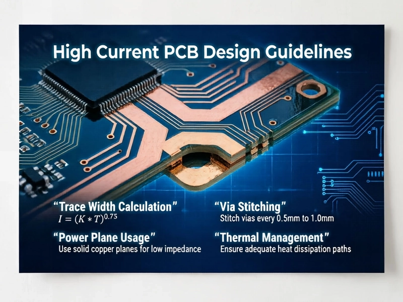
High Current PCB Design Guidelines: Ensuring Reliability and SafetyJune/08/2026
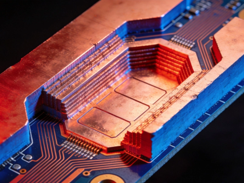
High Current PCB Embedded Copper: Internal vs. External Heat DissipationSeptember/26/2026
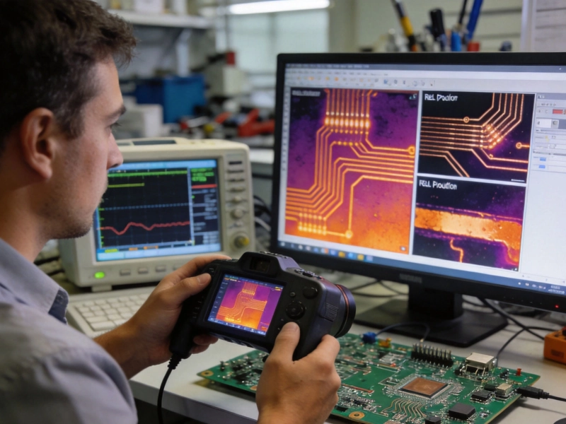
Copper Pour vs Trace: What 3 Years of PCB Failures Taught UsMay/21/2026
High Current PCB Ceramic Substrates: DBC vs. AMB Performance ComparisonOctober/14/2026
High Current PCB Design for Renewable Energy MicrogridsSeptember/30/2026