

Server racks today demand more power than ever before. A single high-density rack can house hundreds of blade servers, storage arrays, network switches, and Power Distribution units that collectively draw tens of kilowatts. At the heart of delivering that power reliably sits the rack-level power supply, a specialized unit that converts AC mains to the DC voltages needed by modern servers: typically 12 volts for most logic, 5 volts for legacy systems, and 3.3 volts for certain peripherals. Designing the PCB for such a power supply is not a task for the faint of heart. You are dealing with currents that can exceed 100 amps, thermal loads that demand active cooling, and a reliability expectation measured in years of continuous operation.
This article walks through the essential considerations for building a High Current Pcb power supply that can meet the demands of modern data center infrastructure. We will cover trace sizing, Thermal Management, component selection, safety isolation, and the layout decisions that separate a working prototype from a production-ready design.
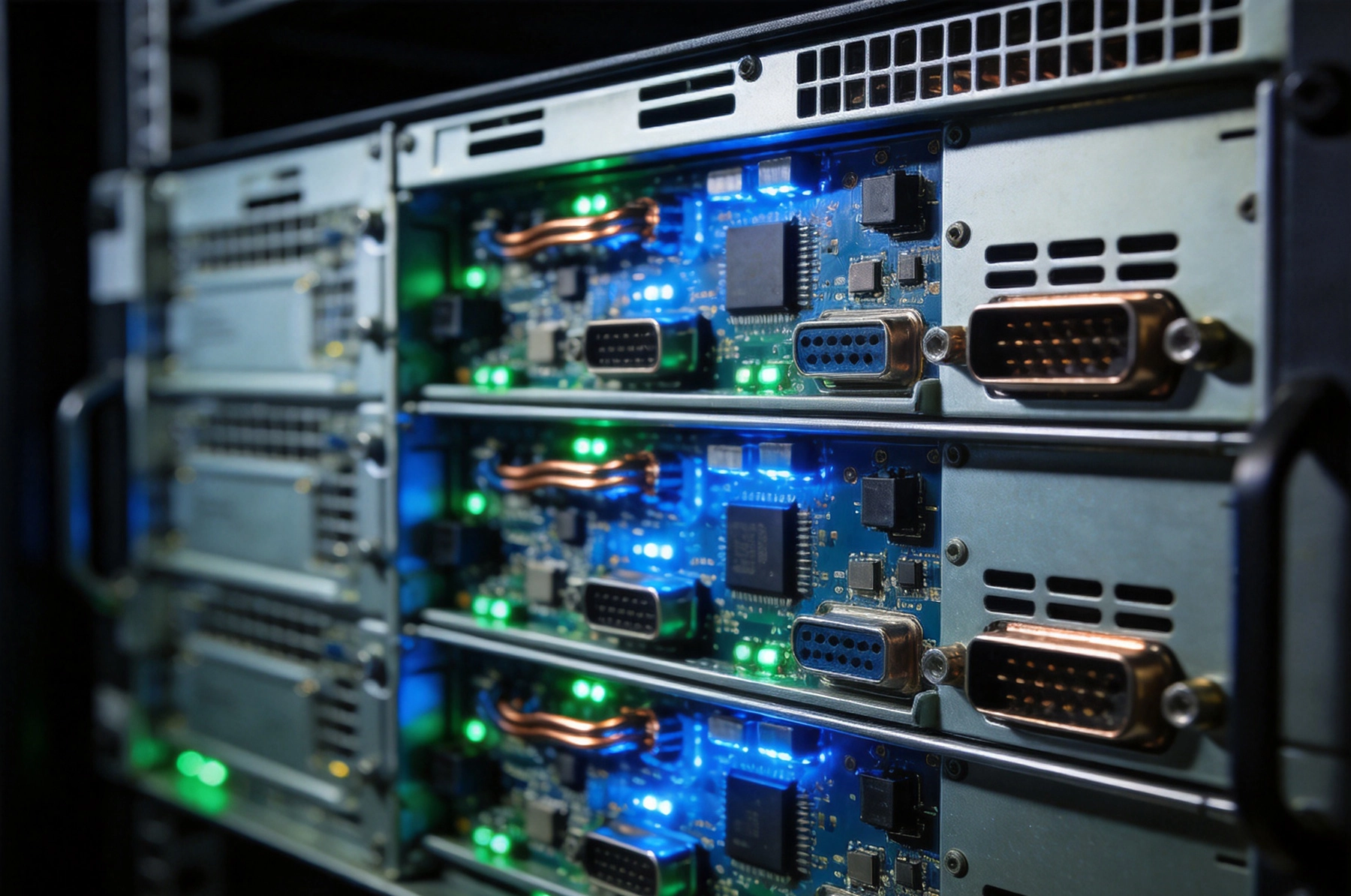
Before placing a single component, you need to characterize what you are actually building. Server rack power supplies typically fall into two categories. AC-DC front-end units convert 208 or 480 volt three-phase AC down to a 12 volt or 48 volt bus. DC-DC intermediate bus converters, or IBCs, step that intermediate voltage down to the final output rails. The Pcb Design challenges differ between these architectures.
For a High Current 12 volt output delivering 2,000 watts, you are looking at sustained currents over 160 amps. Even at 48 volts, a 2,000 watt supply pushes 40 amps, which is still substantial. These current levels dictate everything from trace widths to connector choices to thermal dissipation strategy. Undersizing any single element can create a bottleneck that leads to overheating, voltage drop, or outright failure under load.
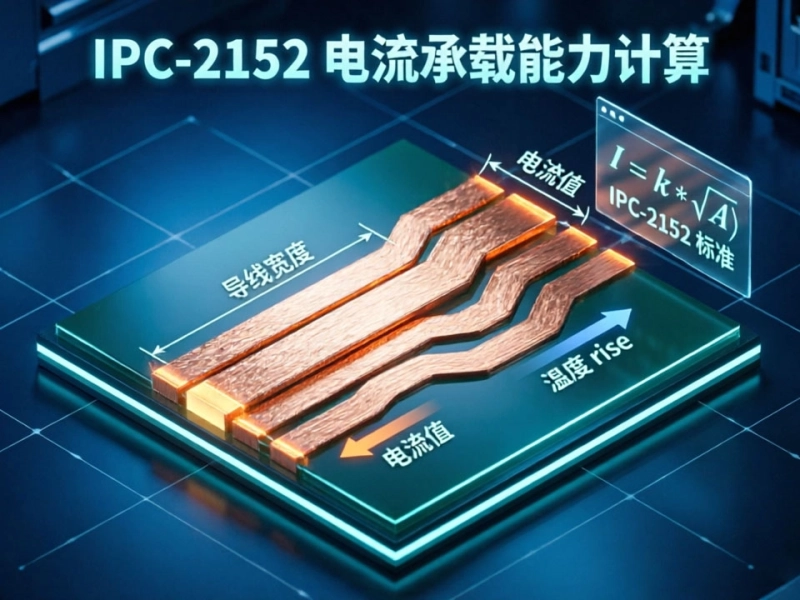
The fundamental equation governing trace width is the Ipc-2152 standard, which replaced the older Ipc-2221 guidelines. Ipc-2152 accounts for modern board materials and provides more accurate thermal modeling than the simplified charts many engineers still use. At its core, the standard relates trace width to Current Carrying Capacity based on temperature rise above ambient.
For a 100 amp trace on standard 2 ounce copper, you might need a trace 40 millimeters wide to keep temperature rise under 20 degrees Celsius. That is wider than many PCB designers are used to seeing. For reference, a standard signal trace on a digital board might be 0.25 millimeters wide. A power trace at 100 amps is literally hundreds of times wider. This reality fundamentally changes how you approach layout.
When board space is tight, increasing Copper Thickness lets you carry more current in a narrower trace. Moving from 2 ounce to 4 ounce copper doubles current capacity for the same width, or lets you halve the width for the same current. Many server power supply designs use 3 to 6 ounce copper on power layers, with some going as heavy as 10 ounces for the main input and output buses.
The tradeoff is manufacturing complexity. Heavy Copper requires different etching processes, and the aspect ratio between Copper Thickness and trace width affects the minimum achievable feature size. You cannot route 4 mil traces reliably on 6 ounce copper. Plan your layer stack carefully, reserving Heavy Copper layers for the Power Planes and using standard weight copper for signal layers.
For very high currents, sometimes a single trace is not enough even with heavy copper. The solution is to run multiple traces in parallel, either on the same layer or distributed across layers. A four-layer board might have the main power bus split between two internal layers, each carrying half the total current. This approach also helps with thermal distribution, spreading the heat load across more copper area.
Every ohm of resistance in a trace or component generates heat. At 100 amps, even 0.001 ohms of trace resistance dissipates 10 watts. Multiply by multiple traces and component resistances, and a power supply PCB can easily generate hundreds of watts of internal heat. Managing that heat is the single biggest challenge in High Current Pcb Design.
Copper is an excellent thermal conductor, which helps spread heat from hotspots across the board. Large copper pours act as heat spreaders, conducting thermal energy away from hot components like MOSFETs and rectifiers toward cooler areas. Strategic placement of Thermal Vias connects these copper pours to internal ground planes or dedicated heat sink layers, creating vertical thermal paths to the board surface.
Hot components need space. Power semiconductors like MOSFETs and Schottky diodes should be placed where they have access to airflow and are not blocked by other large components. Keep electrolytic capacitors away from hot zones, since their lifetime degrades rapidly at elevated temperatures. A capacitor rated for 2,000 hours at 105 degrees might last 5,000 hours at 85 degrees. Given that server power supplies run 24/7, every degree of temperature reduction matters.
Most rack power supplies rely on forced air cooling. The Pcb Layout should align with the airflow path, positioning hot components downstream in the air stream rather than upstream where they heat the air before it reaches other parts. Consider using thermally conductive PCB substrates like aluminum-backed boards for the power stage, which can conduct heat directly to a chassis heat sink without relying solely on air cooling.
MOSFET selection for High Current applications requires balancing on-resistance, switching speed, and thermal characteristics. Lower on-resistance means less conduction loss but often comes with higher gate charge, which increases switching losses. For a 12 volt output at 100 amps, you want MOSFETs with on-resistance in the single-digit milliohm range. Modern silicon MOSFETs and gallium nitride devices can achieve this, though GaN requires more careful gate drive design.
Package selection matters too. DPAK and D2PAK packages have better thermal performance than SO-8 or similar small outlines because they can transfer heat to the board more effectively. For the highest currents, consider directFET or similar packages with exposed metal tabs that solder directly to the PCB for improved thermal coupling.
Input and output capacitors in server power supplies see significant ripple current. Choose capacitors with low equivalent series resistance, or ESR, and rated ripple current that exceeds your expected load. Solid polymer aluminum electrolytics and multilayer ceramic capacitors in parallel are common combinations, with ceramics handling high-frequency ripple and electrolytics providing bulk capacitance.
Inductors for high current designs need cores that do not saturate under peak currents and windings with sufficient copper area to minimize resistive losses. Powdered iron or gapped ferrite cores work well for inductors in the 1 to 100 microhenry range. For very high currents above 50 amps, custom wound toroidal inductors may be necessary to achieve the required current handling and thermal performance.
Do not forget the mechanical interfaces. Input and output connectors must handle the full rated current without excessive heating or voltage drop. Anderson Powerpole, Molex Mega-Fit, and similar high-current connectors are standard in the industry. Screw terminals work for fixed installations but add assembly time. Whatever connector you choose, verify its current rating at the expected operating temperature, as derating curves can be significant.
Server rack power supplies connect to mains voltage. Safety standards like IEC 60950 and UL 60950-1 mandate minimum creepage and clearance distances between primary and secondary circuits. For a 208 volt three-phase input, you typically need 5 to 8 millimeters of clearance depending on the pollution degree and material group. These distances constrain Component Placement and trace routing.
Where the AC input meets the DC output, a reinforced isolation barrier is required. This usually takes the form of a slot cut in the PCB, sometimes with additional insulating material. Optocouplers or digital isolators bridge this barrier for feedback and control signals. Plan your layout to keep high-voltage traces on one side of the barrier and low-voltage circuits on the other, with no components straddling the isolation gap.
Overcurrent protection is mandatory. Input fuses protect against catastrophic failures. Output current limiting prevents damage to the supply and downstream equipment during short circuits. Some designs include foldback current limiting that reduces output voltage as current increases, which limits power dissipation during fault conditions. Place current sense resistors in the ground return path where they can be monitored without high common-mode voltages.
High di/dt loops, like the switching node in a buck converter, generate electromagnetic interference. Minimize the physical area enclosed by these loops by placing input capacitors, switches, and inductors as close together as possible. This reduces both radiated EMI and parasitic inductance that causes voltage overshoot during switching transitions.
When measuring current through a sense resistor, use Kelvin sense connections that tap off directly at the resistor pads, not downstream in the main current path. This eliminates voltage drop in the Pcb Traces from corrupting your Current Measurement. The sense traces can be thin since they carry negligible current, but route them differentially to cancel common-mode noise pickup.
A solid ground plane is essential for both thermal and electrical performance. High current returns should have dedicated ground paths, either as wide traces or as portions of the ground plane segregated from noisy digital grounds. Star grounding techniques, where multiple ground points connect to a single central point, can help isolate switching noise from sensitive control circuits.
A high current power supply PCB cannot be fully validated with simulation alone. Physical testing is essential. Start with low current testing to verify control loop stability and basic functionality. Gradually increase load while monitoring temperatures at critical points: MOSFET cases, inductor windings, capacitor bodies, and connector pins. Infrared thermal imaging is invaluable for spotting hotspots.
Load testing should include transient response to step loads, which stresses the output capacitors and control loop. A server rack supply might see load steps from 10% to 100% in milliseconds as blade servers power cycle. The supply must maintain output voltage regulation within specified limits, typically plus or minus 5%, during these transients.
Server power supplies are expected to last five to ten years in continuous operation. Component derating is essential for achieving this longevity. Running a capacitor at 50% of its voltage rating and well below its maximum temperature rating dramatically extends life. Similarly, MOSFETs operated with substantial margin between normal junction temperature and maximum ratings will outlast those running near their limits.
Design for manufacturability matters too. A layout that requires hand soldering or complex assembly steps increases cost and reduces consistency. Choose component packages that work with standard pick-and-place and reflow processes. Avoid placing large components over small ones, which can create shadowing during reflow and lead to cold solder joints.
Building a High Current Pcb power supply for server racks is a multidimensional engineering challenge that spans Electrical Design, Thermal Management, safety compliance, and manufacturing practicality. Success requires attention to detail at every level, from the width of individual traces to the overall system architecture. The reward is a power supply that can deliver kilowatts of reliable power day after day, year after year, keeping the servers running and the data flowing.
The principles outlined here apply whether you are designing a 500 watt unit for a small rack or a 3,000 watt behemoth for a hyperscale data center. Understand your current requirements. Size your traces and components appropriately. Manage the heat. Respect the safety standards. Do those things, and your power supply will not just work. It will work reliably for the long haul.
For currents above 50 amps, 3 to 6 ounce copper is recommended on power layers. The main input and output buses may benefit from 10 ounce copper or external bus bars. Signal and control layers can use standard 1 ounce copper. Match the Copper Weight to the actual Current Density, using IPC-2152 calculations as a starting point and validating with thermal testing.
Use multiple parallel traces across layers, heavy copper construction, and large copper pours for heat spreading. Keep trace lengths short to minimize resistance. Ensure good thermal coupling between hot traces and Heat Sinks or chassis through Thermal Vias. Active cooling with forced air is typically required for very high current designs.
Modern server power supplies target 94% or higher efficiency at 50% load, with 80 Plus Platinum and Titanium certifications requiring 94% and 96% respectively at that operating point. Efficiency matters because every percentage point of loss becomes heat that must be removed from the data center, impacting cooling costs.
Minimize loop areas in high di/dt circuits. Use proper shielding and filtering on input and output. Keep switching nodes away from sensitive analog circuitry. Implement proper grounding with star grounding for mixed-signal sections. Layout is often more important than filtering for controlling conducted and radiated emissions.
Server power supplies typically require UL, CE, and CB certifications, with testing to IEC 60950-1 or the newer IEC 62368-1 standards. These cover electrical safety, fire enclosure requirements, and isolation barriers. Certification testing should be planned early in the design process, as layout changes required to meet safety standards can be significant.
Building a 50A DC-DC Converter: High Current PCB Layout Lessons LearnedJuly/12/2026
High Current PCB Daisy-Chain vs. Star Routing: Voltage Drop ComparisonAugust/08/2026
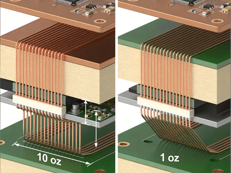
Heavy Copper vs Standard Copper PCB: Complete Comparison Guide for EngineersMay/20/2026
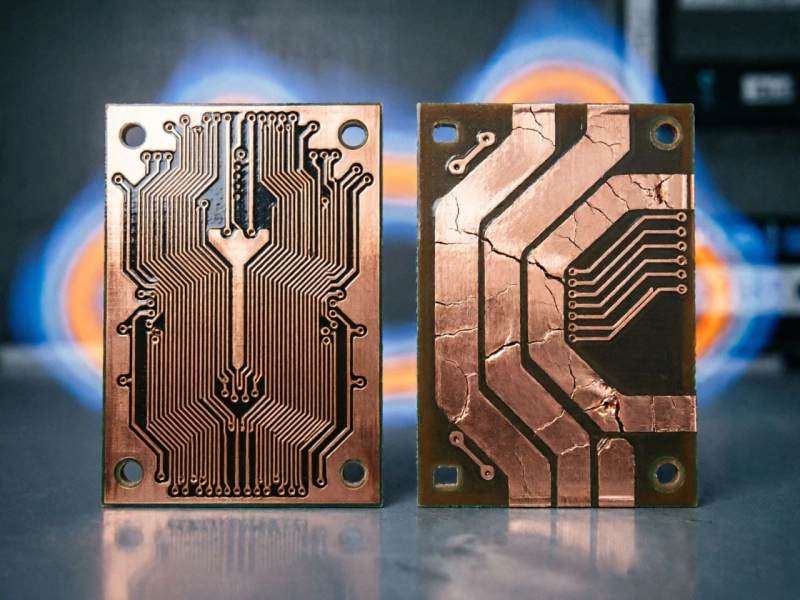
High Current PCB vs. Standard PCB: A Real-World Thermal Stress TestJuly/09/2026
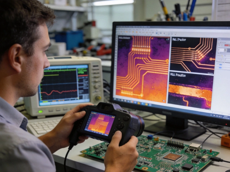
Copper Pour vs Trace: What 3 Years of PCB Failures Taught UsMay/21/2026
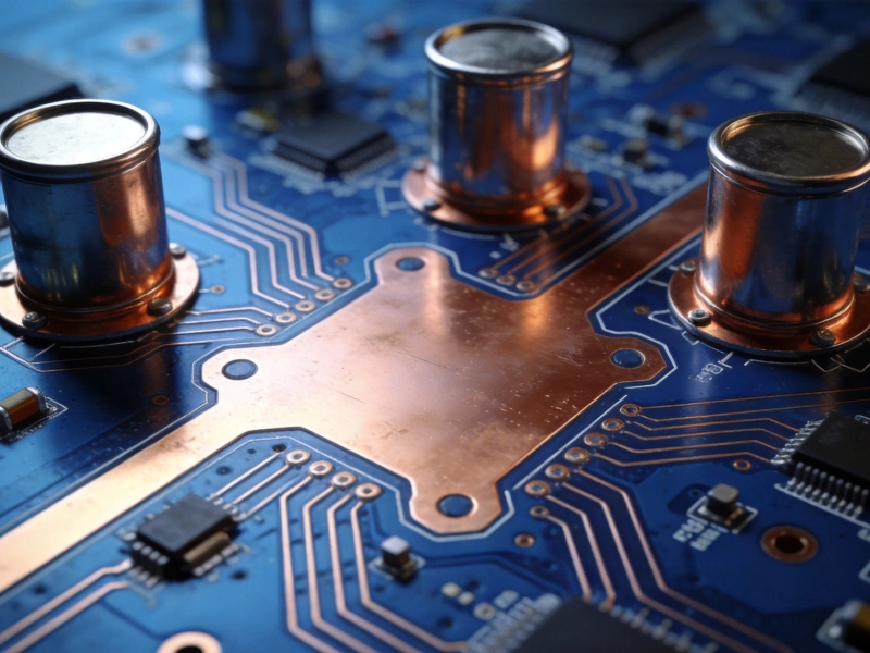
High Current PCB EMI Shielding: Ground Pour vs. Shielding CansAugust/14/2026
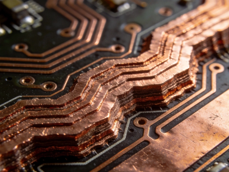
High Current PCB Bus Bars vs. Heavy Copper Traces: Cost and PerformanceJuly/25/2026
Mastering IPC-2152 Current Carrying Capacity Calculation for Reliable PCB DesignJune/04/2026