

High Current PCB design presents unique challenges, with solder wicking into vias being a critical concern during assembly. When solder melts and flows away from component pads into via holes, it creates insufficient solder joints that compromise electrical and mechanical reliability. This article compares tented vias versus untented vias in High Current applications, examining solder wicking mechanisms, design trade-offs, and proven mitigation strategies.
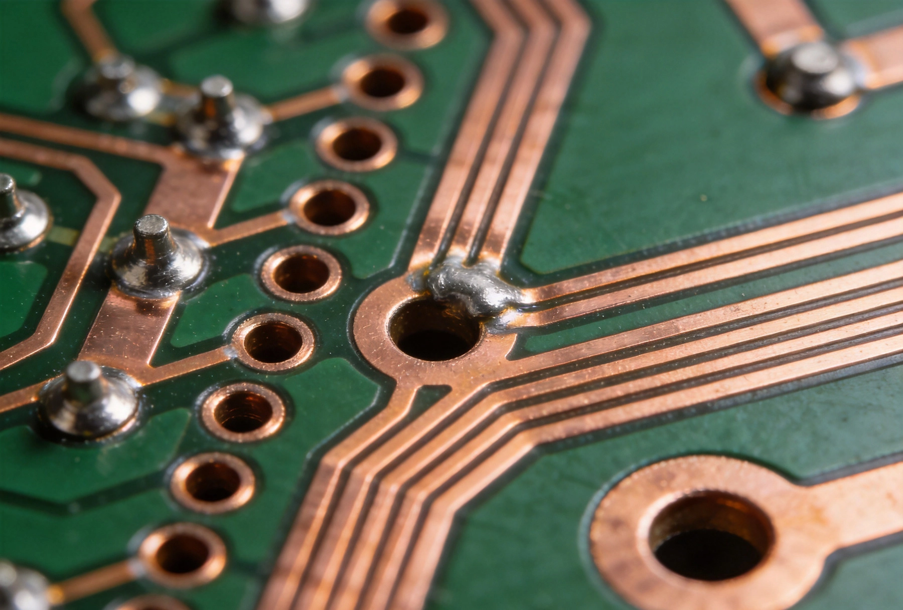
Solder wicking occurs when molten solder migrates from component pads into vias due to capillary action during reflow soldering. The phenomenon is particularly problematic with untented vias where the barrel plating provides a conductive path for solder flow. As solder draws away from the pad surface, the resulting joint may exhibit insufficient solder volume, increased electrical resistance, and reduced mechanical strength.
Capillary forces drive solder wicking, with smaller via diameters experiencing stronger wicking effects due to higher surface tension-to-volume ratios. Via Plating Thickness also influences wicking—thicker plating (typically 1-2oz copper) creates smoother barrel surfaces that facilitate solder flow compared to thinner 0.5-1oz plating. The reflow profile, particularly time above liquidus (TAL), determines how long solder remains molten and susceptible to wicking.
Tented vias are covered with solder mask, preventing solder paste from entering via barrels during assembly. This design effectively eliminates solder wicking by physically blocking solder flow paths. The solder mask covering, typically 10-15µm thick, withstands reflow temperatures and maintains integrity throughout the soldering process.
For High Current applications, tented vias preserve solder at component pads, ensuring adequate joint volume for Current Carrying Capacity. This is critical for power components like MOSFETs, diodes, and current sense resistors where insufficient solder creates localized heating points and potential failure modes. Tented vias also simplify solder paste stencil design, as apertures can match pad dimensions without compensation for via coverage.
However, tented vias present trade-offs. The solder mask coverage adds Thermal Resistance to the via barrel, reducing Heat Dissipation capabilities. In high current circuits, this Thermal Resistance can create hot spots, especially when vias serve as thermal paths between layers. Additionally, tented vias may trap air or flux residues during lamination, potentially causing outgassing during reflow and creating voids in solder joints.
Untented vias remain open through the solder mask layer, allowing direct electrical and thermal connection between layers. This configuration provides superior thermal conductivity, as heat transfers directly through plated via barrels without solder mask insulation. For Power Electronics, untented vias effectively dissipate heat from component pads to inner layer ground planes or heat spreaders.
Electrical resistance in untented vias is lower than tented alternatives, beneficial for high current paths minimizing voltage drop and power loss. The Direct Copper-to-copper connection throughout the via barrel provides maximum Current Carrying Capacity. Designers often specify untented vias for thermal relief pads, current-carrying traces, and ground connections in power supply circuits.
The primary risk is solder wicking, particularly problematic with surface mount components. During reflow, solder paste flows into open via barrels, depleting solder from component pads. This effect is most severe with fine-pitch components, small pads, and vias positioned near pad edges. Insufficient solder joints increase electrical resistance, reduce mechanical strength, and create reliability issues under Thermal Cycling conditions.
Effective High Current PCB design balances Solder Joint Reliability with thermal and electrical performance. Several strategies mitigate solder wicking while maintaining current carrying capabilities.
Positioning vias at safe distances from component pads reduces wicking risk. Industry guidelines recommend minimum spacing of 0.5mm (20 mils) between via centers and pad edges for SMT components. This distance allows solder paste to flow onto pads without reaching via openings. For power components with larger pads, designers may increase spacing to 0.75mm (30 mils) for additional margin.
Via diameter selection influences both wicking risk and current carrying capacity. Smaller vias (0.3mm/12 mil diameter) reduce solder volume loss due to wicking but may increase electrical resistance. Larger vias (0.5-0.8mm/20-30 mil) provide better current capacity but present greater wicking targets. A balanced approach uses 0.4mm/16 mil vias for most high current applications, offering adequate current handling with moderate wicking risk.
Partial tenting provides an intermediate solution, covering via openings near component pads while leaving Thermal Vias exposed for Heat Dissipation. This approach preserves solder at critical pads while maintaining thermal performance in less critical areas. Design software typically supports selective tenting via solder mask expansion settings applied on a per-via basis.
Via plugging fills via barrels with solder mask or epoxy after fabrication, preventing solder wicking while maintaining thermal performance. Plugged vias cost more than standard tented vias but provide superior protection against solder ingress. IPC-4761 defines multiple plug types, including Type V (full via fill) offering complete protection against solder wicking and flux entrapment.
Solder paste selection impacts wicking behavior. Higher viscosity pastes (Type 4 or Type 5) resist capillary flow into vias more effectively than lower viscosity alternatives. Pastes with larger alloy particles (Type 3, 25-45µm) also reduce wicking compared to fine-pitch pastes (Type 5, 15-25µm) designed for small components.
Stencil aperture design compensates for potential solder loss by increasing paste volume on pads with nearby vias. Aperture expansion of 10-15% relative to pad dimensions ensures adequate solder remains after wicking. For vias positioned closer than recommended distances, stencil designers may incorporate additional paste islands bridging pad edges to replenish wicking losses.
PCB Fabrication quality directly influences solder wicking behavior. Consistent Via Plating Thickness, smooth barrel surfaces, and clean Solder Mask Application all affect how solder flows during assembly. Manufacturers must control via plating to IPC-6012 specifications, ensuring minimum 1oz copper plating with consistent coverage throughout the barrel.
Solder Mask Application requires precise registration to achieve reliable tenting. Misaligned solder mask may leave via openings partially exposed, creating paths for solder wicking while complicating assembly. High-quality fabrication houses implement vision systems to align solder mask layers within ±25µm of design specifications, ensuring complete via coverage where required.
Assembly process optimization includes reflow profiling tailored to prevent excessive solder wicking. Reducing time above liquidus (TAL) to 45-60 seconds limits solder flow into vias while still achieving proper joint formation. Peak temperature control (typically 235-245°C for Lead-free Solder) prevents excessive solder fluidity that accelerates wicking. Nitrogen atmospheres with oxygen levels below 50 ppm improve solder joint quality without increasing wicking risk.
Implementing these proven strategies minimizes solder wicking while optimizing High Current Pcb performance:
For power supply applications, consider using dedicated Thermal Vias separate from signal vias. Thermal vias positioned under component pads remain untented for heat dissipation, while signal vias use tenting to preserve solder at component connections. This dual approach optimizes both thermal performance and Solder Joint Reliability.
X-ray inspection provides the most reliable method for detecting solder wicking defects. X-ray imaging reveals solder distribution within via barrels and confirms adequate joint volume at component pads. Automated X-Ray Inspection (AXI) systems can detect solder wicking with >95% accuracy, identifying issues before assemblies proceed to testing.
Cross-section analysis validates via fill quality and solder joint integrity. Sample boards undergo destructive testing to measure solder joint thickness, verify complete via tenting, and assess thermal performance. Cross-section data guides process improvements and validates design modifications for future production runs.
Electrical testing detects resistance increases associated with insufficient solder joints. Four-wire Kelvin measurements on high current paths identify solder wicking issues that increase series resistance beyond design specifications. Thermal imaging under load conditions reveals hot spots indicating inadequate current carrying capacity due to solder wicking defects.
Solder wicking represents a significant reliability concern in High Current Pcb Design, particularly with untented vias positioned near component pads. Tented vias effectively prevent wicking but introduce thermal resistance that may compromise power circuit performance. The optimal design approach balances solder joint reliability with thermal and electrical requirements through strategic via placement, selective tenting, and optimized assembly processes.
Successful High Current Pcb implementation requires collaboration between design engineers, PCB fabricators, and assembly partners. Early engagement enables material selection, via design optimization, and process qualification before production begins. By understanding solder wicking mechanisms and implementing proven mitigation strategies, designers create high current PCB assemblies that deliver reliable performance throughout product lifecycles.
High Current PCB Grounding: Star Ground vs. Ground Plane in High Current PathsJuly/31/2026
Overcoming Voltage Drop in High Current PCB Power Planes: A Case StudyJuly/13/2026
High Current PCB Surface Finish: ENIG vs. HASL for High Current PadsSeptember/23/2026

High Current PCB Ceramic Substrates: DBC vs. AMB Performance ComparisonOctober/14/2026
High Current PCB Routing: 45-Degree Angles vs. Curved Traces in PracticeJuly/12/2026
High Current PCB Current Crowding: Sharp Corners vs. Teardrop TransitionsSeptember/03/2026
Designing a 100A High Current PCB for EV Battery Management SystemsJuly/09/2026
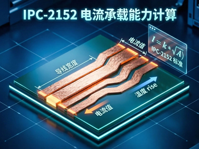
Mastering IPC-2152 Current Carrying Capacity Calculation for Reliable PCB DesignJune/04/2026