

Power Electronics designers face critical Thermal Management decisions when dealing with High Current PCB applications. Choosing between thermal interface pads and direct copper exposure for heat sink attachment significantly impacts thermal performance, assembly complexity, and long-term reliability. Understanding each approach's characteristics helps engineers optimize designs for specific application requirements.
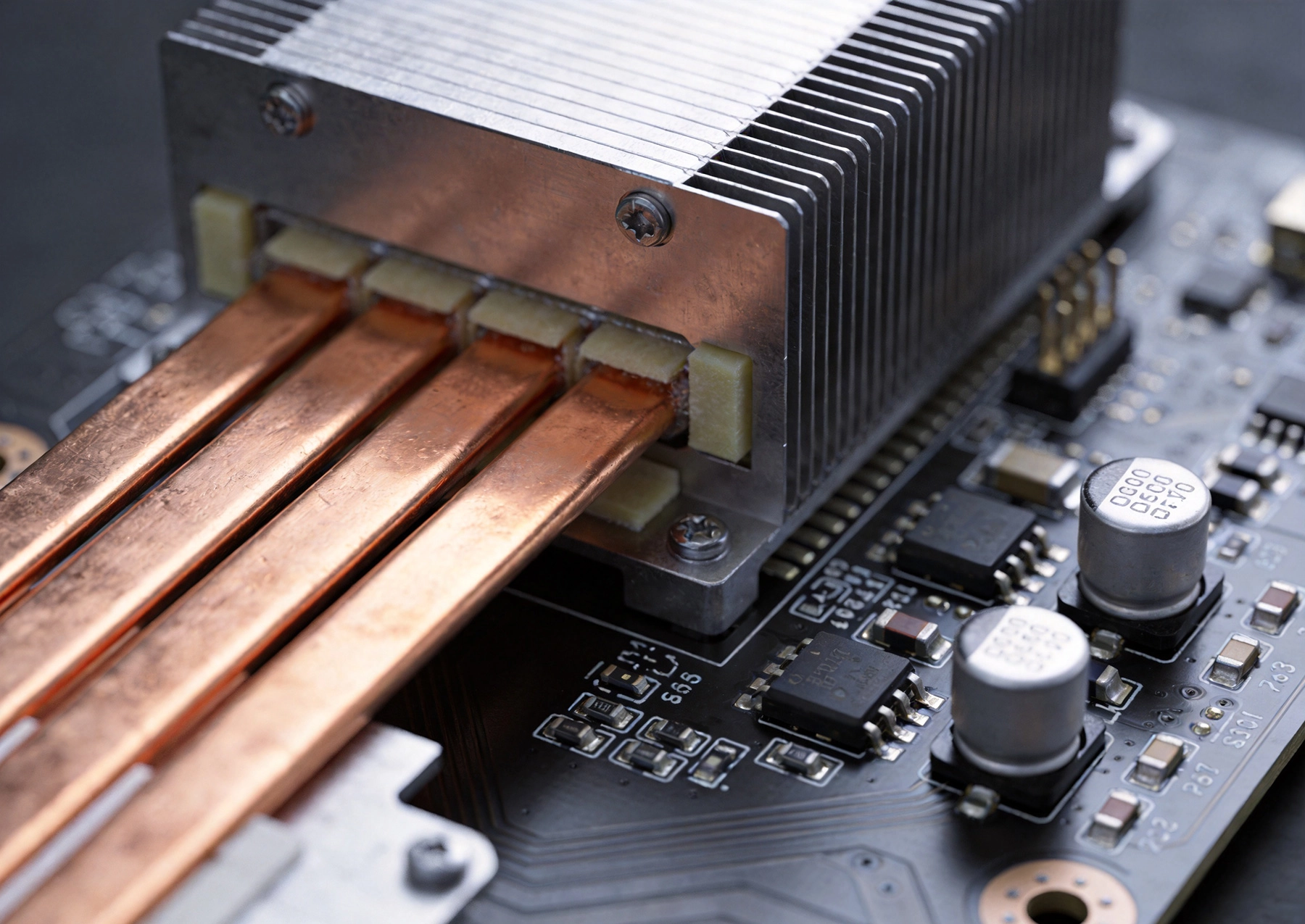
High Current PCBs generate substantial heat through resistive losses in traces, component junctions, and interconnects. A trace carrying 20A with 10mΩ resistance dissipates 4W continuously. Multiple power paths and switching components compound thermal loads, creating hotspots that can exceed component ratings or cause premature failures.
Traditional cooling approaches use attached Heat Sinks to increase surface area for convection and radiation. However, transferring heat from PCB copper to aluminum or copper Heat Sinks introduces Thermal Resistance at the interface. Minimizing this resistance becomes critical for maintaining safe operating temperatures.
Two primary interface methods dominate High Current applications: thermal interface pads that conform to surface irregularities, and direct copper exposure where heat sinks attach directly to board copper without intermediate layers. Each approach offers distinct advantages depending on application priorities.
Thermal pads provide compliant layers that fill microscopic gaps between PCB surfaces and heat sink mounting faces. These materials range from silicone-based gap fillers to ceramic-filled elastomers, offering various thermal conductivity ratings from 1W/mK to over 6W/mK.
Thermal pads function by displacing air from the interface region. Air's thermal conductivity of approximately 0.026W/mK creates substantial resistance to heat flow. Even thin air gaps dramatically increase overall Thermal Resistance. Thermal pads replace air with materials offering 40-200 times better conductivity.
The conformal nature of thermal pads accommodates surface roughness, flatness variations, and mounting pressure inconsistencies. This compliance ensures contact across the entire interface area, preventing localized hot spots that might occur with rigid attachments.
Surface tolerance accommodation allows thermal pads to compensate for Pcb Warpage from uneven copper distribution or reflow stresses. Heat sinks with machining variations also mate effectively with compliant interfaces.
Electrical isolation comes standard with most thermal pad materials. Silicone-based pads provide dielectric strength exceeding 5000V, protecting grounded heat sinks from live circuit potentials. This eliminates need for additional insulation layers.
Assembly simplicity reduces manufacturing complexity. Thermal pads can be applied manually or with pick-and-place equipment, requiring no special surface preparation beyond standard cleanliness.
Rework capability permits heat sink removal and reinstallation. Pads can be replaced if assemblies require service, though care must prevent contaminant introduction during reassembly.
Interface resistance remains the primary drawback. Even premium thermal pads add 0.1-0.5°C/W thermal resistance depending on thickness and material conductivity. For high power density applications, this additional resistance might prove unacceptable.
Material degradation concerns arise in high-temperature or high-humidity environments. Silicone oils can migrate, causing contamination risks. Some pad materials harden or become brittle after extended Thermal Cycling, reducing compliance over time.
Thickness constraints affect both thermal resistance and mechanical stability. Thinner pads improve thermal performance but reduce ability to accommodate surface variations. Designers must balance competing requirements.
Direct copper exposure eliminates intermediate layers by creating bare copper regions on PCB surfaces where heat sinks mount. Copper surfaces mate directly with heat sink bases, minimizing interface resistance through precision machining and controlled flatness.
Solder mask removal in designated thermal zones exposes underlying copper. Standard PCB Fabrication processes can define these areas during mask application. However, exposed copper oxidizes over time, potentially increasing contact resistance.
Gold plating over exposed copper provides oxidation protection and improves surface flatness. Enig (Electroless Nickel Immersion Gold) surfaces offer excellent thermal contact characteristics while maintaining solderability for potential component attachment.
Covered copper areas without solder mask can be specified during Pcb Design. These regions receive full Copper Thickness plus surface plating, creating robust thermal interfaces capable of sustained pressure loading.
Minimal thermal resistance represents the primary benefit. Eliminating intermediate material layers reduces interface resistance to near-zero values determined by Surface Finish and contact pressure. This approach suits extreme power density applications.
Long-term stability improves without organic materials that might degrade. Metal-to-metal interfaces maintain consistent characteristics over product lifetime, avoiding concerns about pad aging or material migration.
Thermal Cycling performance benefits from the stable interface. Direct copper contacts withstand thermal expansion cycling without compliance loss. This reliability matters for automotive, industrial, and aerospace applications experiencing wide temperature ranges.
Surface flatness requirements demand precision machining of heat sink mounting surfaces. Any warpage or irregularity creates air gaps that the interface cannot fill. This requires tighter manufacturing tolerances and potentially more expensive heat sinks.
Electrical connectivity between PCB copper and heat sink creates design constraints. Heat sinks must be isolated or designed to accept circuit potentials. This complicates grounding strategies and might require insulated heat sink variants.
Assembly precision requirements increase without compliant materials. Mounting pressure must be uniform across the interface, requiring careful torque control and often multiple fasteners to ensure even contact pressure distribution.
Corrosion risk exists for unprotected copper surfaces. Exposure to humidity, contaminants, or corrosive atmospheres degrades contact surfaces over time. Protective plating adds cost and requires process control.
Thermal resistance comparison illustrates the performance gap between approaches. Consider a 50mm x 50mm thermal interface area transferring 25W:
Thermal pad interface with 0.5mm thick, 3W/mK conductivity material creates approximately 0.17°C/W thermal resistance. For 25W Heat Dissipation, the pad itself contributes 4.25°C temperature rise. This becomes significant when junction temperatures approach maximum ratings.
Direct copper interface with properly prepared surfaces achieves thermal resistance below 0.05°C/W. The 25W load produces less than 1.25°C temperature rise across the interface, representing 3°C improvement over thermal pad solutions.
However, these calculations assume ideal conditions. Real-world factors like mounting pressure variations, surface contamination, and assembly inconsistencies modify actual performance. Thermal pad compliance often masks assembly variations that direct copper approaches expose.
Total cost analysis must weigh material costs against manufacturing complexity, yield implications, and reliability investments.
Thermal pad material costs range from $0.10 to $2.00 per interface depending on material grade, thickness, and area. Premium ceramic-filled materials command higher prices but offer better thermal performance. Volume procurement reduces per-unit costs substantially.
Direct copper surface preparation adds PCB Fabrication cost through mask removal operations or specialized plating. Heat sink machining for flatness increases component cost. Assembly labor for precision mounting adds production expense.
Yield impact differs between approaches. Thermal pads tolerate assembly variations, producing consistent yields. Direct copper interfaces might suffer yield losses from surface contamination, mounting pressure inconsistency, or tolerance accumulations.
Rework costs favor thermal pad approaches. Failed assemblies can be disassembled, cleaned, and rebuilt with new interface material. Direct copper interfaces might require PCB replacement if surfaces become damaged or contaminated during disassembly.
Selecting the optimal approach requires evaluating application requirements against each method's characteristics.
Consumer electronics typically favor thermal pads for cost efficiency and assembly simplicity. Product lifecycles of 2-5 years don't challenge thermal pad longevity. Electrical isolation simplifies design and reduces bill-of-materials complexity.
Industrial equipment often specifies thermal pads for serviceability. Field maintenance scenarios benefit from forgiving interfaces that tolerate some assembly variation. Moderate power densities don't demand ultimate thermal performance.
Automotive applications require careful evaluation. Thermal cycling demands might favor direct copper for long-term stability. However, electrical isolation requirements often mandate thermal pads. Hybrid approaches using insulated heat sinks with direct copper contact address both concerns.
Telecommunications and data center equipment with high power density frequently employs direct copper interfaces. Maximum thermal performance enables higher component density and reduced cooling system size. Controlled environments minimize corrosion and contamination concerns.
Aerospace and defense applications typically specify direct copper or advanced thermal interface materials with documented reliability. Mission-critical equipment cannot risk thermal interface degradation over extended service lives.
Successful implementation requires attention to design details beyond interface material selection.
Thermal via arrays connecting inner copper layers to interface surfaces improve heat spreading. Via density of 1-2 per square centimeter with 0.3mm diameter provides effective thermal coupling to internal planes.
Copper area sizing should account for Current Distribution and heat spreading. Interface areas larger than component footprints spread thermal load, reducing localized heating. Design copper areas 1.5-2x component contact dimensions where space permits.
Mounting pressure specifications ensure consistent interface contact. Thermal pad manufacturers specify minimum compression requirements. Direct copper interfaces benefit from higher pressure, typically 20-50 PSI across the interface area.
Fastener placement significantly affects pressure distribution. Multiple fasteners surrounding thermal interfaces produce more uniform pressure than single central mounting. Finite element analysis helps optimize fastener patterns for specific geometries.
Surface Finish specifications for direct copper should call out flatness requirements. Specifying 0.05mm maximum flatness deviation ensures adequate contact without excessive machining costs.
Thermal pads and direct copper exposure represent complementary approaches to High Current PCB Thermal Management, each suited to different application priorities. Thermal pads offer assembly simplicity, electrical isolation, and rework capability at the cost of additional thermal resistance. Direct copper interfaces maximize thermal performance and long-term stability while demanding precision manufacturing and Electrical Design accommodation.
Designers should evaluate power density requirements, environmental conditions, reliability expectations, and cost constraints when selecting interface methods. Consumer and industrial applications often benefit from thermal pad simplicity, while high-power-density and long-life applications might justify direct copper's precision requirements.
Hybrid approaches combining both techniques might suit specific applications. Insulated heat sinks with direct copper contact provide electrical isolation without thermal pad resistance. Selective use of thermal pads in critical areas while employing direct copper elsewhere optimizes thermal performance against isolation requirements.
Work closely with PCB fabricators and assembly partners to specify appropriate surface finishes, flatness requirements, and assembly procedures. Proper implementation ensures chosen thermal interface approaches deliver expected performance throughout product lifetime.
Standard thermal interface pads range from 1-3W/mK for silicone-based materials. Premium ceramic-filled pads achieve 4-6W/mK or higher. Thermal conductivity directly affects thermal resistance—doubling conductivity halves interface resistance for equivalent thickness.
Thermal pad thickness typically ranges from 0.25mm to 1.0mm for PCB heat sink applications. Thinner pads improve thermal performance but reduce tolerance to surface variations. Choose minimum thickness that accommodates expected flatness variations while maintaining consistent contact.
Direct copper exposure transfers heat from surface copper to heat sinks but doesn't replace Thermal Vias for internal layer heat extraction. Thermal Vias remain necessary for conducting heat from inner layers and component thermal pads to interface surfaces.
Thermal pads should be replaced if heat sinks are removed for service. Used pads may not provide consistent contact upon reinstallation due to compression set and potential contamination. Always specify replacement thermal pads in service procedures.
Higher mounting pressure improves thermal contact for both pad and direct copper interfaces. Thermal pads require minimum compression to achieve rated thermal resistance—typically 10-20% of pad thickness. Direct copper interfaces benefit from maximum pressure that doesn't damage surfaces, improving metal-to-metal contact area.
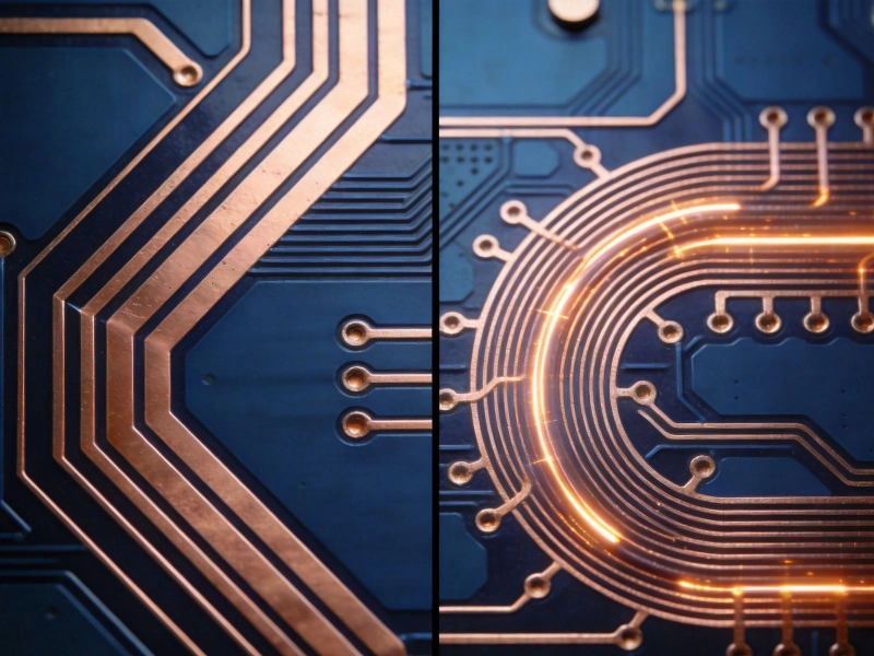
High Current PCB Routing: 45-Degree Angles vs. Curved Traces in PracticeJuly/10/2026
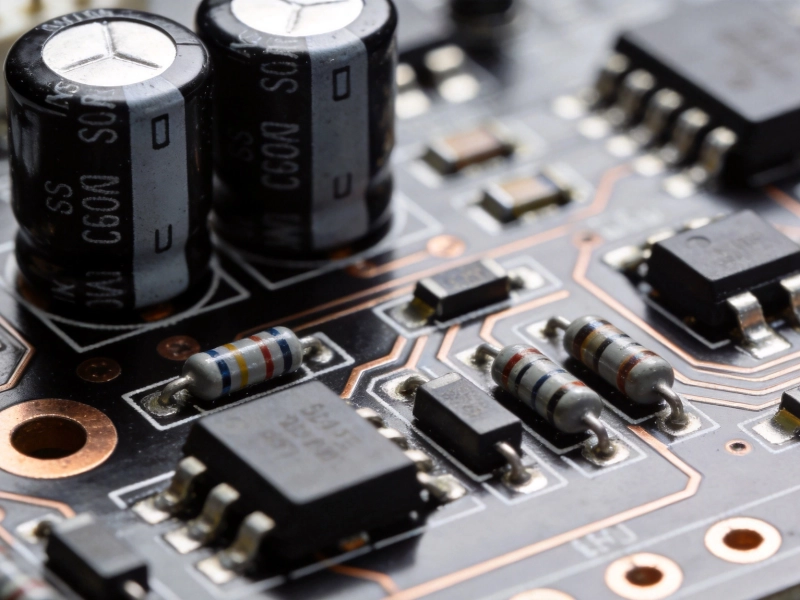
High Current PCB Snubber Circuits: Placement Impact on Voltage SpikesAugust/06/2026
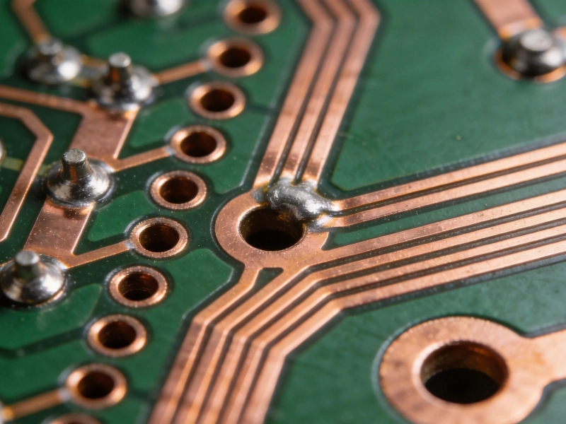
High Current PCB Solder Wicking: Tented Vias vs. Untented ViasSeptember/01/2026
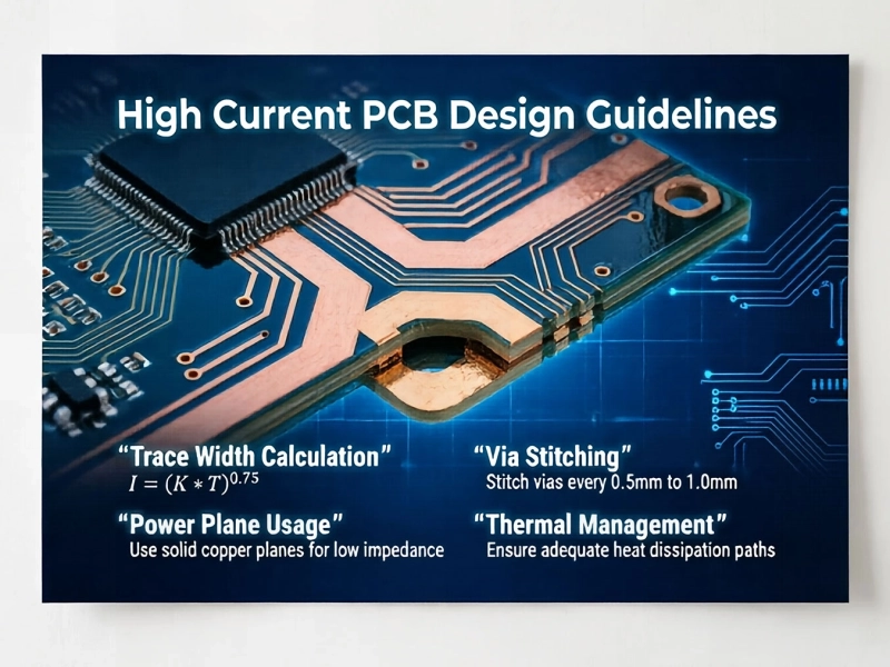
High Current PCB Design Guidelines: Ensuring Reliability and SafetyJune/08/2026
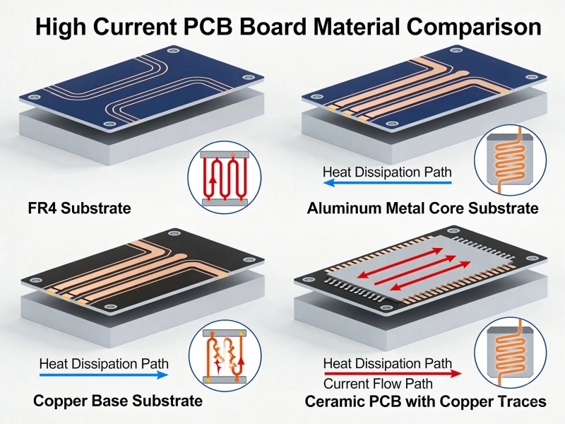
Best Material for High Current PCB Design: How to Choose the Right SubstrateJune/05/2026
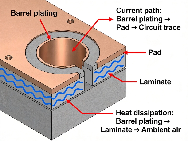
Plated Through Hole Current Rating for PCBsJune/10/2026
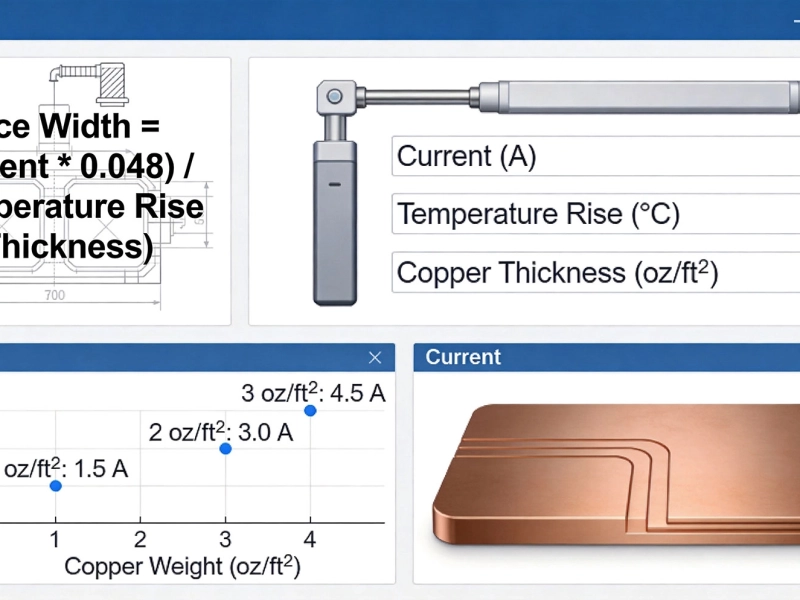
High Current PCB Trace Width Calculator: The Ultimate Engineering GuideMay/20/2026
High Current PCB Design for Drone ESCs: Minimizing Loop InductanceAugust/03/2026