
Power Electronics push PCB technology to its limits. When currents climb into the tens or hundreds of amps, design flaws that would be invisible in low-power circuits become catastrophic failures. High Current PCBs fail in ways that standard Pcb Design intuition fails to predict—traces open unexpectedly, solder joints crack under thermal stress, entire board regions delaminate from overheating. Understanding how and why High Current PCBs fail transforms guesswork into engineering confidence. This knowledge separates designs that survive field deployment from prototypes that fail in the engineering lab.
Chinese manufacturers have extensive experience with High Current Pcb failures, having built Power Electronics for applications ranging from electric vehicle chargers to industrial motor drives. This manufacturing experience reveals patterns—common mistakes that appear repeatedly across different designs and different customers. Learning from these documented failures prevents reinventing the wheel, saving engineering time while avoiding the embarrassment and cost of field failures.
This comprehensive guide examines the primary failure modes affecting high current PCBs, explains the mechanisms driving each failure type, and provides actionable prevention strategies. Whether you're designing your first power electronics board or seeking to improve reliability of established products, this information helps you create designs that perform reliably under real-world stress conditions.
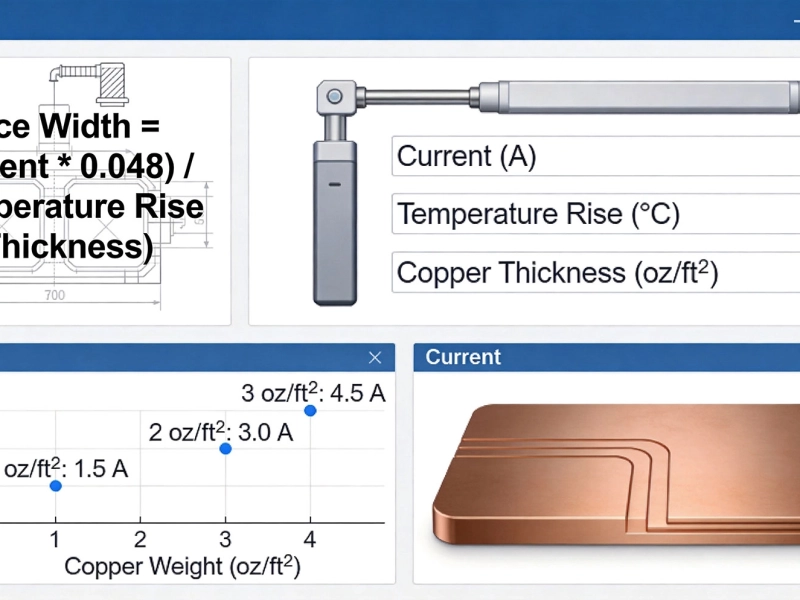
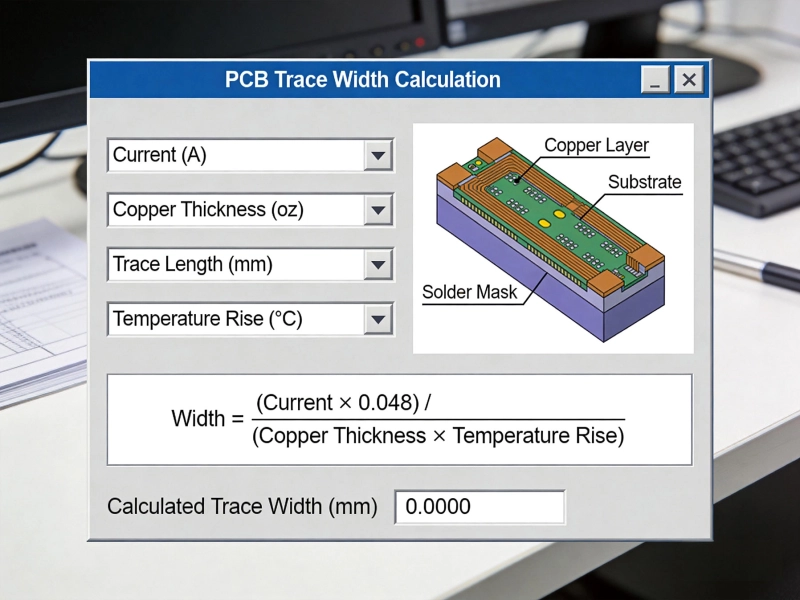
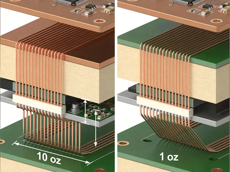
PCB Trace Current Capacity follows basic physics—copper resistance generates heat as current flows, and that heat must dissipate to prevent excessive temperature rise. The relationship between current and temperature rise depends on trace geometry, Copper Thickness, ambient conditions, and board construction. Many PCB designers rely on simplified tables or calculator tools without understanding the underlying assumptions, leading to designs that fail when assumptions don't match reality.
External factors dramatically affect Trace Current Capacity. Trace width calculators typically assume still air and moderate thermal relief. High-current traces in enclosed enclosures with limited airflow may carry far less current than calculated before overheating. Adjacent high-power components heat nearby traces, reducing their current capacity below calculated values. Vias serving as current paths have different thermal characteristics than surface traces—calculators that ignore Via Current Capacity may underestimate heating in current-carrying via arrays.
Derating practices provide safety margins against unknown factors. Conservative engineering applies derating factors of 50% or more to calculated current capacity, ensuring reliable operation despite calculator limitations and unknown environmental conditions. When your calculations suggest a trace handles 30 amps, designing for 15 amps provides margin against the numerous factors calculators cannot capture. This margin costs board area but prevents field failures.
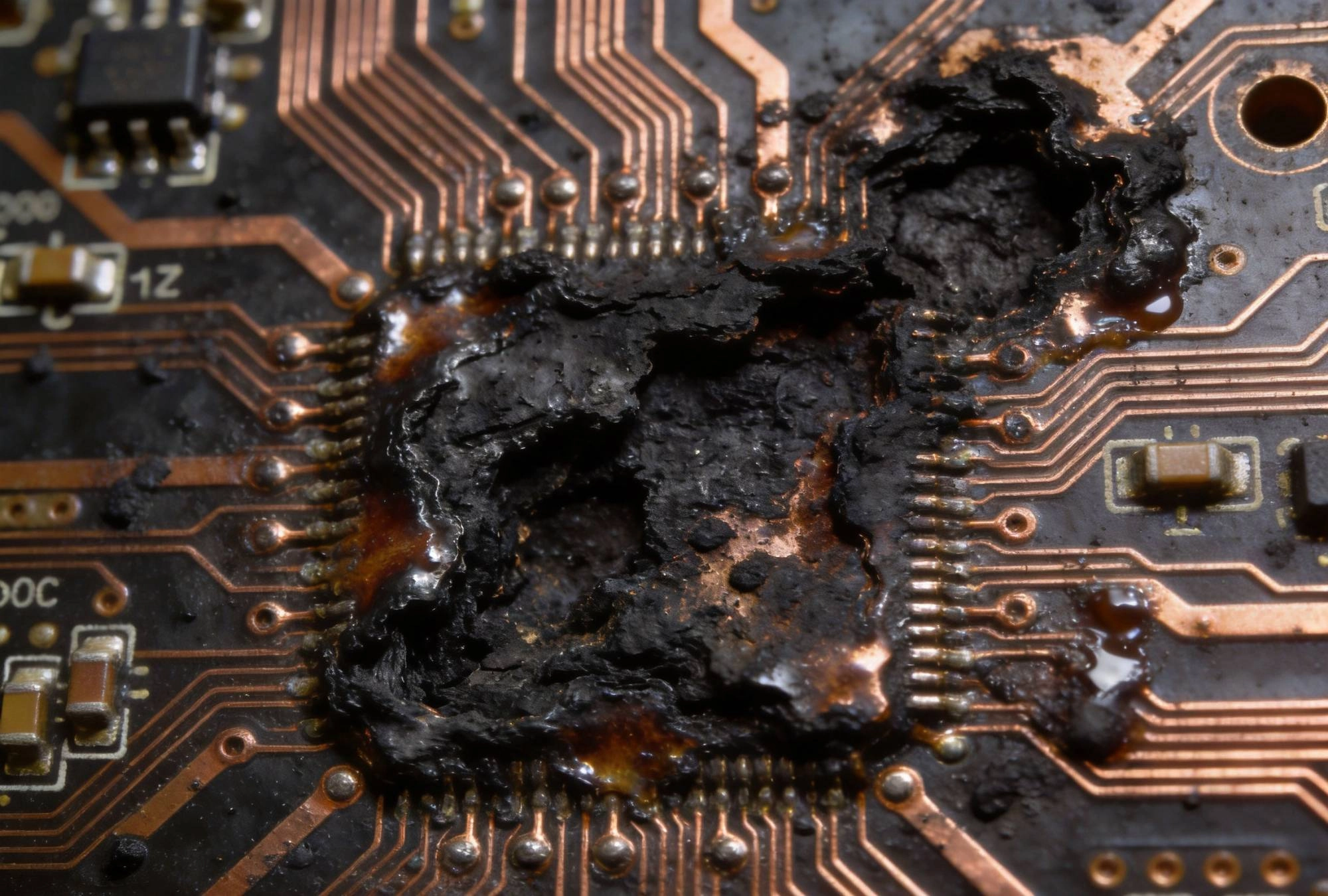
Electromigration represents a fundamental failure mechanism in high-current Pcb Traces. When electrons flow through metal conductors, they transfer momentum to metal atoms, gradually pushing atoms in the direction of electron flow. At high current densities—typically exceeding 10,000 amps per square centimeter—electromigration becomes significant. Over months or years, this atomic movement creates voids in trace areas where current density peaks, eventually opening circuits without warning.
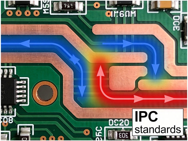
Current crowding at geometric discontinuities accelerates electromigration dramatically. Trace corners, transitions between trace widths, and via entries create local current density peaks where electromigration concentrates. Straight traces with smooth corners experience less electromigration stress than traces with sharp 90-degree bends. Designing high-current paths with gradual transitions and wide radii reduces current crowding that drives electromigration failure.
Prevention strategies address electromigration through design choices. Wider traces reduce current density directly. Thicker copper reduces current density without increasing trace width. Avoiding sharp corners and geometric discontinuities eliminates current crowding. Adding redundant current paths provides safety against localized failures. Board-level coatings can suppress electromigration by preventing surface atom migration, though this approach adds cost and complexity.
High current operation creates thermal cycles that accumulate damage over time. Power dissipation causes heating; current removal allows cooling; this thermal cycling repeats with every power cycle or load change. Each thermal cycle produces small plastic deformation as materials expand and contract at different rates. Over thousands or millions of cycles, this accumulated damage manifests as cracked solder joints, delaminated pads, and fractured trace-to-plating interfaces.
Solder joint fatigue follows predictable patterns. High-current components generate heat that cycles the joint between operating temperature and ambient. The coefficient of thermal expansion mismatch between component, solder, and PCB substrate drives cyclic plastic deformation. Eventually fatigue cracks propagate through the joint, increasing resistance until the connection fails intermittently or completely. Larger components with higher thermal mass create larger temperature excursions and more severe fatigue stress.
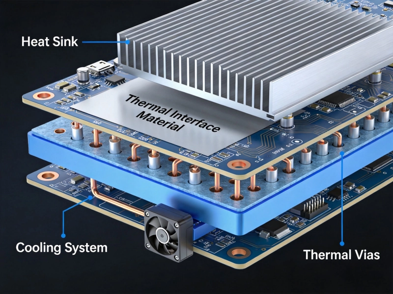
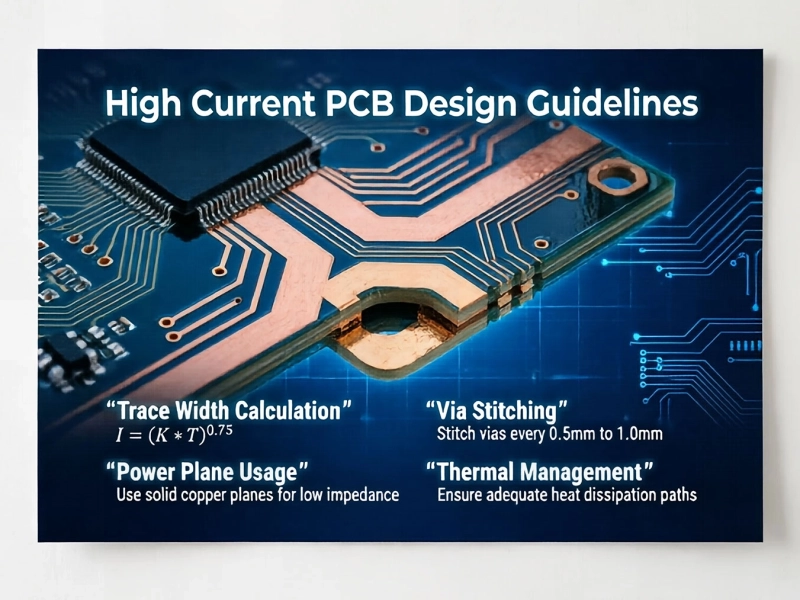
Via-in-pad constructions face particular thermal fatigue challenges. Thermal Vias connecting component pads to internal planes conduct heat away efficiently during operation, but this same thermal path creates steep thermal gradients across the joint during power cycling. The concentrated thermal cycling in via-in-pad structures accelerates fatigue in surrounding solder joints. Careful design of thermal via density, pad size, and solder mask opening balances Thermal Management against fatigue life.
Vias carrying high current present unique thermal challenges. The barrel surface area determines current capacity, but barrel heating occurs primarily at the barrel walls where current density concentrates. Plating quality affects Via Current Capacity substantially—voids, voids, or thin plating in barrel walls create hot spots that accelerate failure. Chinese manufacturers vary significantly in their plating process control; verifying your manufacturer's plating quality prevents via-related field failures.
Via arrays distributing current across multiple vias reduce individual via heating proportionally. Ten vias sharing 100 amps each carry 10 amps per via versus 100 amps in a single via. However, current distribution in via arrays depends on trace routing that connects to the array—poor routing may leave some vias carrying more current than others, defeating the paralleling benefit. Careful routing ensures equal current sharing across all vias in high-current arrays.
Thermal via placement affects component reliability significantly. Components dissipating substantial power benefit from Thermal Vias positioned under their thermal pads. However, placing thermal vias too close to signal vias can affect signal integrity, and excessive thermal vias can weaken the pad structure mechanically. The optimal thermal via pattern balances thermal performance against mechanical reliability and manufacturing constraints.
Connectors represent common failure points in high-current systems. The interface between Pcb Traces and connector contacts involves multiple material transitions and mechanical interfaces, each presenting potential failure modes. Contact resistance at the connector interface generates heat proportional to current squared—doubling current quadruples heating at the contact interface. This heating accelerates contact degradation, creating a vicious cycle that eventually leads to connection failure.
Connector current ratings assume specific conditions that may not match your application. Manufacturers specify current ratings based on controlled testing with stable environmental conditions. In practice, vibration, thermal cycling, and corrosion can degrade connector performance well below rated current. Applying connector ratings at face value without derating invites failures from environmental stress that testing conditions don't capture.
Termination design for high-current PCB-to-wiring interfaces requires attention to mechanical stress. Wire crimps and solder terminations create stress concentrations where wires enter terminations. Vibration and thermal cycling flex wires, transmitting fatigue stress to the termination joint. Strain relief mechanisms prevent wire movement from stressing terminations. Your termination design should accommodate the mechanical environment your product will experience.
High-temperature operation causes PCB material degradation that weakens structural integrity. Standard FR-4 laminates experience moisture absorption, resin degradation, and glass transition effects when operated near their temperature limits. Power electronics can easily exceed FR-4's maximum operating temperature in localized areas, creating thermal gradients that drive delamination between board layers.
Thermal expansion mismatch between copper and substrate creates stress at copper-to-substrate interfaces. High-current heating amplifies this stress, eventually separating copper from substrate in a process called "trace lifting." Traces lifting from the substrate may remain electrically connected through thin copper bridges, creating intermittent failures that are notoriously difficult to diagnose. Proper adhesion promotion during PCB fabrication prevents this failure mode.
Metallurgical changes in PCB plating affect long-term reliability. High-temperature exposure causes grain growth in copper plating, reducing strength over time. Tin-lead and lead-free finishes undergo intermetallic compound formation at elevated temperatures. These metallurgical changes occur gradually, meaning boards may pass initial testing but fail after months of field operation. Understanding the metallurgical behavior of your plating choices helps predict long-term reliability.
High current density in solder joints generates localized heating that affects joint integrity. The resistive heating in narrow solder joints can approach temperatures that approach the solder melting point during extreme current spikes. While normal operation shouldn't approach these conditions, fault conditions and transient overloads create current surges that stress joints beyond normal design limits.
Solder composition affects high-current performance. Some solder alloys handle high-current stress better than others due to differences in electrical resistivity, thermal conductivity, and mechanical properties. Lead-free solders generally have higher resistivity than tin-lead alloys, generating more heat at equivalent current density. Selecting solder alloys optimized for power electronics applications provides margin against current-related joint stress.
Manufacturing defects that might be acceptable in low-power circuits become critical in high-current applications. Voids in solder joints create localized current crowding that accelerates both heating and electromigration. Solder voids exceeding 20% of joint area significantly reduce current capacity and mechanical strength. X-ray inspection revealing excessive voids predicts premature failure in high-current applications.
Conservative trace width selection provides the foundation for high-current reliability. Rather than designing to the theoretical limit of your calculator, apply substantial safety margins. Doubling or tripling calculated trace widths costs board area but provides insurance against the numerous factors your calculations cannot capture. This margin also accommodates future modifications that might increase current requirements without requiring board redesign.
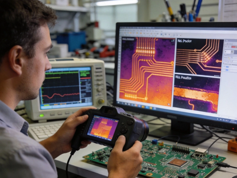
Thermal simulation during design identifies hotspots before boards are manufactured. Thermal imaging of prototype boards reveals whether designs meet thermal expectations. This feedback loop iterates toward improved designs, eventually producing boards with adequate thermal margin. Skipping prototype testing to save time often extends project timelines when thermal problems surface during qualification testing or field deployment.
Component selection considers thermal performance alongside electrical specifications. Components with excellent electrical ratings but poor thermal dissipation create localized heating that stresses surrounding traces and joints. Selecting components that move heat efficiently reduces board-level thermal challenges. Heat Sinks, thermal pads, and forced air cooling extend the thermal capability of component choices.
Chinese PCB manufacturers vary significantly in their capability for high-current boards. Copper Thickness consistency affects current capacity directly; inconsistent plating creates hot spots where copper is thinner than nominal. Verify your manufacturer's process control for plating thickness uniformity—XRF measurements on sample boards reveal actual consistency versus stated specifications.
Thermal Management during assembly affects high-current board reliability. The multiple thermal cycles of lead-free assembly stress solder joints more severely than leaded processes. Some manufacturers offer thermal profiles optimized for high-reliability applications; others apply standard profiles regardless of application. Requesting specialized thermal profiles costs more but produces more robust assemblies.
Quality inspection for high-current boards should exceed standard requirements. Standard electrical testing verifies connectivity but doesn't evaluate current-carrying capacity or thermal performance. Requesting extended testing—including thermal imaging under load conditions or current cycling stress testing—validates that manufacturing processes produced boards meeting design intent. This investment in qualification testing prevents field failures.
Design verification testing confirms that prototypes meet current-carrying requirements under realistic conditions. Apply rated current to traces and measure temperature rise with thermal imaging. Verify that temperature rise remains within design limits while accounting for worst-case ambient temperature. This testing reveals whether design margins are adequate and identifies hot spots requiring design modifications.
Accelerated life testing simulates field aging in compressed timeframes. Current cycling, thermal cycling, and powered aging expose designs to stress that would accumulate over years of field operation. Statistical analysis of accelerated test results predicts Field Reliability with quantifiable confidence. This testing investment is mandatory for high-reliability applications like automotive, medical, or industrial systems.
Failure analysis of prototype and production samples reveals weakness that testing might miss. Cross-sectioning reveals internal defects like voids, delamination, and plating problems. Microscopic examination of solder joints identifies manufacturing defects. Thermal imaging during operation shows temperature distribution. This analytical feedback continuously improves design and manufacturing processes.
High Current Pcb failure modes follow predictable patterns that informed designers can prevent. Trace degradation from electromigration, thermal fatigue in solder joints, via current capacity limits, and material degradation all threaten high-current designs. Understanding the mechanisms driving each failure mode enables targeted prevention strategies that address root causes rather than symptoms.
Conservative design practices—generous trace widths, derating factors, and thermal margins—provide the foundation for reliable high-current designs. These practices may seem wasteful during design, but they prevent field failures that cost far more than the additional board area or component cost they require. Prevention truly is more economical than failure.
Manufacturing quality directly affects high-current reliability. Working with Chinese manufacturers who understand high-current requirements and maintain appropriate process controls produces boards that meet design intent consistently. Verifying manufacturing quality through inspection and testing confirms that processes delivered what your design specified. This verification investment protects against failures that field deployment would reveal too late.
How to Reduce Temperature Rise in Power PCBJune/17/2026
How Much Current Can a PCB Trace Carry? Complete Engineering GuideMay/20/2026
High Current PCB Design Guidelines: Ensuring Reliability and SafetyJune/08/2026
High Current PCB Trace Width Calculator: The Ultimate Engineering GuideMay/20/2026
High Current PCB Trace Width Calculator: Complete Guide with Formulas and ExamplesMay/20/2026
Copper Pour vs Trace: What 3 Years of PCB Failures Taught UsMay/21/2026
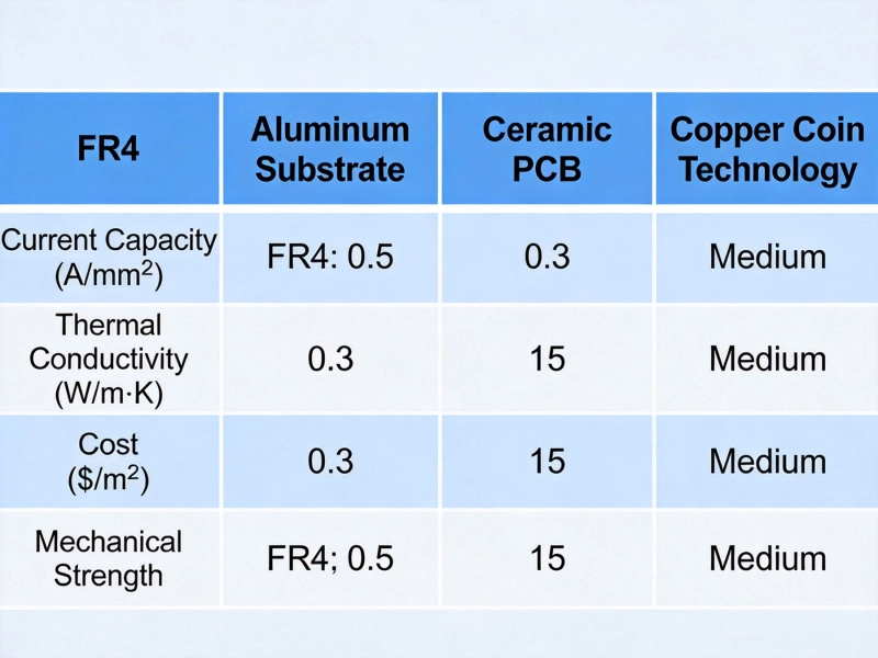
Best Material for High Current PCB DesignMay/21/2026
Heavy Copper vs Standard Copper PCB: Complete Comparison Guide for EngineersMay/20/2026