

Panelization is a practical necessity in PCB production. Individual boards are too small and fragile to handle efficiently through the fabrication and assembly process, so manufacturers combine multiple boards into panels that can be processed as single units and separated afterward. For most PCB applications, choosing between V-score and tab-route panelization is a straightforward decision based on board size, quantity, and Component Placement. For Heavy Copper PCBs carrying high currents, the decision becomes more complex because the mechanical and thermal characteristics of thick copper dramatically affect how each panelization method performs. Making the wrong choice leads to cracked boards, damaged components, or assembly problems that are expensive to debug and correct. Understanding how Heavy Copper changes the panelization calculus helps engineers and project managers specify panelization correctly from the start.
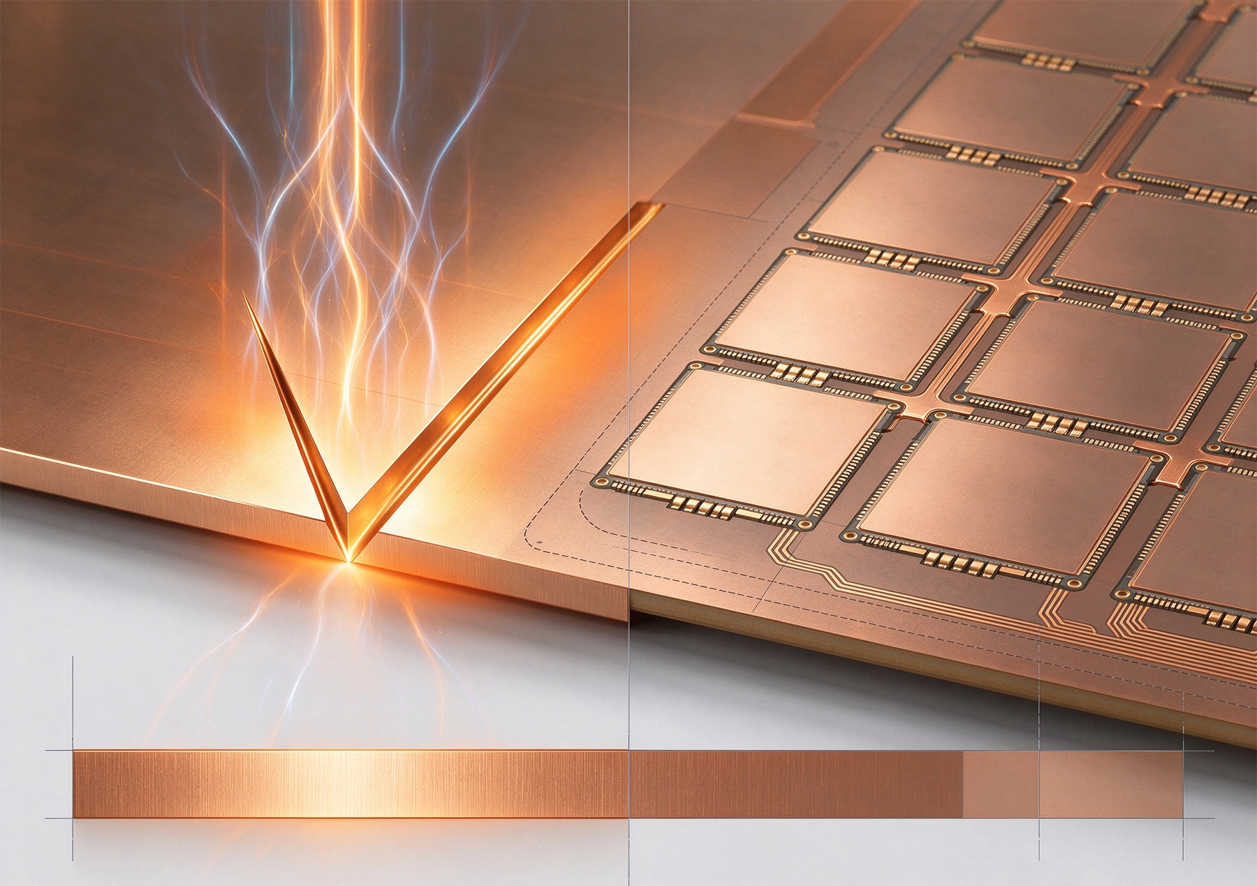
Standard PCB Copper Thickness is 1 ounce per square foot, which corresponds to approximately 35 microns or 1.4 mils. Heavy copper boards typically use 3 ounces or more, with some Power Electronics applications reaching 6 ounces, 10 ounces, or even thicker. The mechanical and thermal properties of the finished board change substantially as Copper Thickness increases, and these changes directly affect how V-score and tab-route panelization perform.
Thick copper creates a board with significantly different flexibility characteristics than thin-copper boards. The copper itself is much stiffer than the substrate material, so a board with 4-ounce copper is substantially more rigid than the same board with 1-ounce copper. This increased rigidity reduces the board's ability to flex at panelization grooves or tabs, which changes the stress distribution during depanelization and affects how cleanly the board separates from the panel.
Thermal mass during assembly is also affected by heavy copper. Boards with thick copper traces absorb more heat during reflow soldering, which can cause uneven heating and different thermal expansion behavior compared to thin-copper boards. If the panelization method introduces stress concentrations from the score or tab geometry, these stress points may interact with thermal gradients during assembly in ways that cause cracking or delamination.
The cross-section of the board edge after separation is different for heavy copper boards. A V-score cuts through the substrate material but leaves copper continuous along the score line, creating stress concentrations at the copper-substrate interface when the board is flexed to separate. With thick copper, this copper remnant is larger and creates more pronounced stress concentration, making the board more susceptible to crack propagation along the edge.
V-scoring is a panelization method where a V-shaped groove is machined into the panel from both sides, leaving a small amount of material at the center of the board to hold the individual boards together until depanelization. The score depth is typically set to leave 20 to 30 percent of the board thickness as the remaining web, though heavy copper boards may require different specifications. After assembly is complete, boards are separated by flexing along the score line, either manually or with automated depaneling equipment.
The V-score process is fast and cost-effective because it requires only a single machining operation per score line. Scores can be cut in seconds, and the panelization setup time is minimal compared to tab-route which requires more complex tooling. For high-volume production of simple rectangular boards, V-score is usually the lowest-cost panelization option.
The main limitation of V-score is that it works best with straight-line separations and requires adequate board flexibility at the score location to separate cleanly. Boards with components mounted near the score line may be damaged if the depanelization force transmits to the component. Boards with heavy copper also create larger stress concentrations at the score web as discussed above, which can lead to edge cracking over time or during handling.
V-score is not suitable for boards with connectors or components that protrude into the score area, because the score groove physically occupies space along the panelization line. Boards must be designed with adequate clearance from score lines to any component or feature that would interfere with the score tooling or the depanelization process.
Tab-route panelization uses a routing tool to cut out the board profiles while leaving small tabs or bridges of material connecting each board to the surrounding panel frame. These tabs are typically spaced at regular intervals along each separation edge and are narrow enough to be broken by hand or with simple tooling after assembly is complete. Unlike V-score which creates a continuous groove, tab-route creates a discontinuous connection that is easier to break cleanly.
The tab-route process is more time-consuming than V-scoring because the routing tool must follow the full perimeter of each board in the panel. For panels with many boards, the total routing time can be substantial. However, tab-route offers much greater flexibility in board shape and panelization layout, allowing non-rectangular boards, boards with cutouts, and complex panel arrangements that would be impossible with V-score.
Tab-width design is critical for the balance between panel integrity during assembly and clean separation afterward. Too narrow a tab and the panel may break during handling or assembly. Too wide a tab and separation becomes difficult and may cause stress damage to the board. For heavy copper boards, tab width typically needs to be larger than for thin-copper boards because the thicker copper and increased board rigidity make the tabs more prone to cracking during separation.
Heavy copper boards present specific challenges for V-score panelization that must be understood and addressed in the panelization specification. The most fundamental issue is that the copper along the score line is not cut by the V-score tooling, so a continuous strip of copper runs along the score axis of each separated board. With heavy copper, this uncut copper strip creates a significant stress concentration at the board edge.
When the board is flexed to separate along the V-score, the uncut copper strip at the bottom of the groove acts as a hinge that concentrates bending stress at the copper-substrate interface. Over time, Thermal Cycling or mechanical stress can cause cracks to initiate at this interface and propagate into the board. Boards with 4-ounce or thicker copper are particularly susceptible to this failure mode, and the problem worsens as the score depth increases beyond optimal levels.
Score depth control becomes more critical with heavy copper because the mechanical advantage of the V-shape depends on creating a controlled hinge point at the remaining web. If the score is too shallow, the web is too thick and the board will not separate cleanly, requiring excessive force that can damage components or the board itself. If the score is too deep, the web is too thin and may break during assembly handling before depanelization is intended. Heavy copper boards may require deeper total cut to achieve the same web thickness, but this deeper cut must be controlled precisely to avoid going all the way through.
Some manufacturers recommend against V-score for boards with copper thickness above 3 ounces, particularly for boards that will see Thermal Cycling or mechanical stress in the end application. The risk of edge cracking may be acceptable for boards that are assembled once and used in benign environments, but for Power Electronics that experience temperature swings or vibration, tab-route is generally the safer choice.
Tab-route panelization handles heavy copper more gracefully because the separation mechanism does not create the same stress concentration at the copper-substrate interface. When tabs are broken to separate a board from the panel, the break occurs through the tab material itself rather than along a groove that leaves uncut copper intact. This means the stress is distributed differently and the copper at the board edge is not forced to act as a bending hinge.
The discontinuous nature of tab connections is actually beneficial for heavy copper boards. Instead of one continuous groove with a continuous copper strip, the tab design creates separate break points where the board can separate cleanly without accumulating stress along the entire edge. The number and spacing of tabs can be adjusted to control the break force and minimize stress on any single tab.
Tab-route also allows the copper to be routed away cleanly at the board edge, rather than leaving a continuous copper strip as V-score does. A routing tool cuts through the copper and substrate equally, so the board edge after separation has no stress concentration at the copper interface. For boards where edge quality and long-term reliability matter, this clean edge is a significant advantage.
The trade-off is that tab-route is slower and more expensive than V-score. For heavy copper boards where the panel quantity is large enough that V-score would be cost-effective, the additional cost of tab-route may be justified by the improved reliability. For lower quantities or prototype runs, the cost difference may be less significant than the schedule impact of the slower routing process.
In some cases, a hybrid approach combining elements of both V-score and tab-route can optimize the trade-offs for heavy copper panels. One common hybrid approach uses tab-route for the panelization edges where heavy copper is present and V-score only for internal panelization between boards where the copper is lighter or absent.
Another hybrid approach uses pre-scoring with thinner webs and tab-break for the final separation. The score creates a partial groove that reduces the material cross-section and makes tab breaking easier, while the remaining tab material provides the structural continuity needed during assembly. This approach requires careful process development to get the score depth and tab width optimized for the specific board construction.
Mouse bites, a variant of tab-route where small circular perforations are used instead of rectangular tabs, offer another option for heavy copper. Mouse bites create multiple small stress concentration points rather than one continuous tab, which can distribute the break force more evenly and reduce the risk of crack propagation. However, mouse bite tooling is specialized and not all manufacturers offer this option.
The method used to separate boards from panels after assembly affects which panelization approach works best. Manual depanelization by hand is the simplest but creates the highest risk of damage, particularly for heavy copper boards where the separation force is higher. Automated depaneling equipment can apply controlled force and displacement to separate boards more consistently.
For V-scored panels, automated depanelizers use a blade or plow to press into the score groove and separate the boards with controlled force. These machines can be configured for specific score depth and board thickness, and they apply the separation force at a controlled rate that reduces the risk of component damage or board cracking. For heavy copper boards, the higher separation force required means the depanelizer must have adequate capacity and the score specification must be appropriate for the heavier copper.
For tab-route panels, depanelization can be done manually by breaking tabs, with a router tool that cuts the remaining tabs, or with specialized tab-breaking equipment that applies controlled bending force to break the tabs cleanly. The choice depends on the tab width, material thickness, and production volume. Higher volumes benefit from automated depanelization regardless of the method, because manual depanelization introduces variability that increases the risk of defects.
Following specific design guidelines for heavy copper panelization reduces the risk of problems during depanelization and in the field. These guidelines account for the mechanical characteristics of heavy copper boards and the practical capabilities of panelization and depanelization processes.
Specify tab-route panelization for copper weights of 3 ounces or greater whenever edge reliability or thermal cycling is a concern. The additional cost compared to V-score is usually modest relative to the total board cost, particularly for power electronics where the Copper Weight is already a significant cost driver. If V-score is required by cost or schedule constraints, discuss the specific Copper Weight and application requirements with the manufacturer to assess the risk and determine if any additional process controls are needed.
Design panelization clearance that accounts for the routing tool diameter for tab-route or the score head width for V-score. Standard clearance from the panelization line to the nearest component is typically 3 to 5 millimeters, but heavy copper boards with high stiffness may benefit from larger clearance to reduce the risk of stress transmission from depanelization to components. Connectors and tall components near panelization lines are particularly vulnerable to damage from depanelization forces.
Consider the board orientation within the panel for depanelization accessibility. If the panel will be depanelized by hand, the break direction should be accessible from the panel edge. If automated depanelization will be used, ensure the panel fits the equipment's working envelope and that the break lines are aligned with the equipment's motion axes. Some automated depanelizers can only apply force in specific directions, which constrains the panelization layout options.
Panelization decisions should be made in collaboration with your PCB manufacturer because the specific capabilities and limitations of their equipment affect what panelization approaches are practical. Sharing information about copper weight, board thickness, Component Placement, and application requirements allows the manufacturer to recommend the most appropriate panelization method and specification.
Request a panelization drawing from the manufacturer that shows the exact score depth, tab width, or other panelization geometry they propose for your board. Review this drawing against your component placement to verify that adequate clearance exists and that no components are placed in locations that would interfere with panelization or depanelization. This review catches potential problems early, before manufacturing tooling is set up and difficult to change.
Ask about first article inspection of panelization results before committing to production. The manufacturer should be able to provide a sample panel that demonstrates the panelization quality, including the cleanliness of separated edges, the integrity of any remaining web material, and the absence of cracks or delamination. For heavy copper boards, this first article inspection is particularly valuable because it reveals any issues with the stress concentration at the panelization line before production of all units begins.
Panelization for heavy copper PCBs requires more careful consideration than panelization for standard boards, because the thicker copper changes the mechanical behavior of the board and the stress distribution at panelization features. V-score works acceptably for some heavy copper applications but creates stress concentrations at the copper-substrate interface that can lead to edge cracking over time or under thermal cycling. Tab-route provides cleaner separation and eliminates the stress concentration problem, making it the preferred choice for boards where reliability is important and copper weight is 3 ounces or greater.
The additional cost of tab-route panelization is usually modest compared to the overall cost of heavy copper board fabrication, and the reliability improvement is substantial for applications where boards will see thermal cycling, vibration, or mechanical stress. Investing in the right panelization approach from the start avoids field failures and the cost of root cause investigation and rework that follow them.
Contact us to discuss your requirements and explore how appropriate panelization methods can support your High Current PCB needs.
High Current PCB Layer Stackup: Symmetrical vs. Asymmetrical Power PlanesJuly/20/2026
High Current PCB Embedded Copper: Internal vs. External Heat DissipationSeptember/26/2026
Cost Comparison: 2oz vs 4oz Copper PCB — What You Need to KnowJune/26/2026
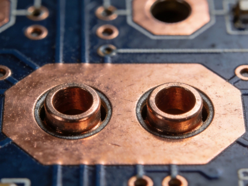
High Current PCB Mounting Holes: Plated vs. Non-Plated for Current ReturnSeptember/29/2026
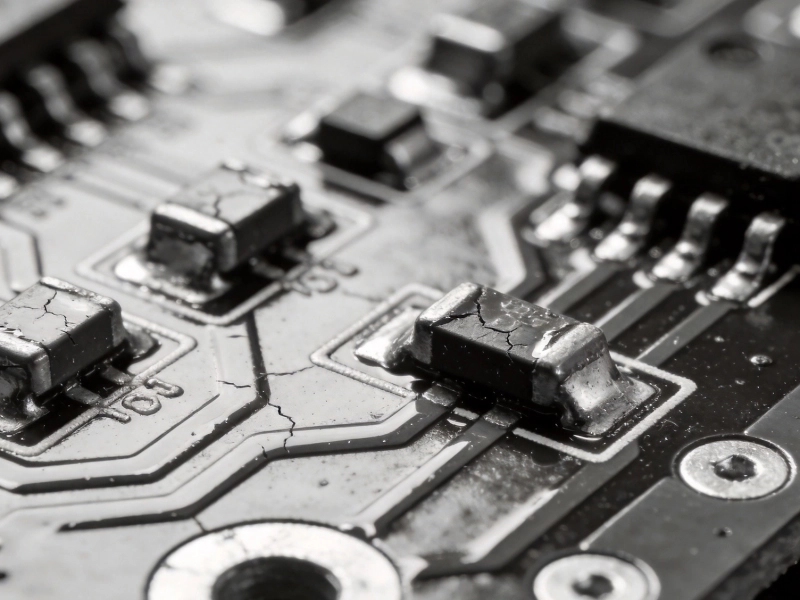
High Current PCB Conformal Coating: Protecting Solder Joints Under Thermal StressAugust/06/2026

Building a 50A DC-DC Converter: High Current PCB Layout Lessons LearnedJuly/12/2026
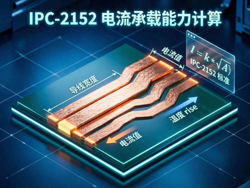
Mastering IPC-2152 Current Carrying Capacity Calculation for Reliable PCB DesignJune/04/2026
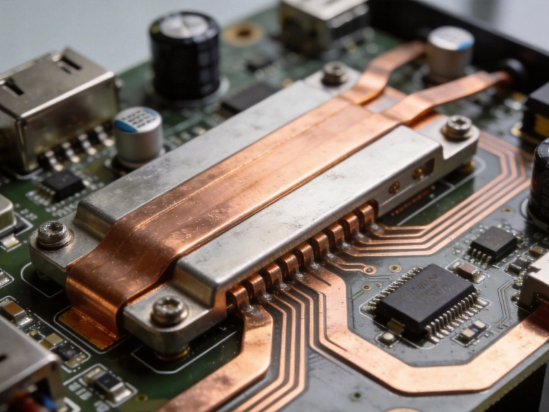
High Current PCB Design for Electric Vehicle Charging StationsAugust/15/2026