

In Power Electronics, managing heat is as important as managing current. A trace that can carry 20 amps on paper may fail in practice if the heat generated by I²R losses cannot escape the board fast enough. This is where the choice between internal embedded copper and external Heavy Copper becomes a critical design decision. Both approaches increase the copper cross-section available for current flow, but they differ fundamentally in how they dissipate heat — and those differences determine which approach works best for a given application.
This article examines the thermal mechanics of internal versus external copper in High Current PCBs, compares their Heat Dissipation performance, and provides guidance on when each approach is the right choice for your power design.
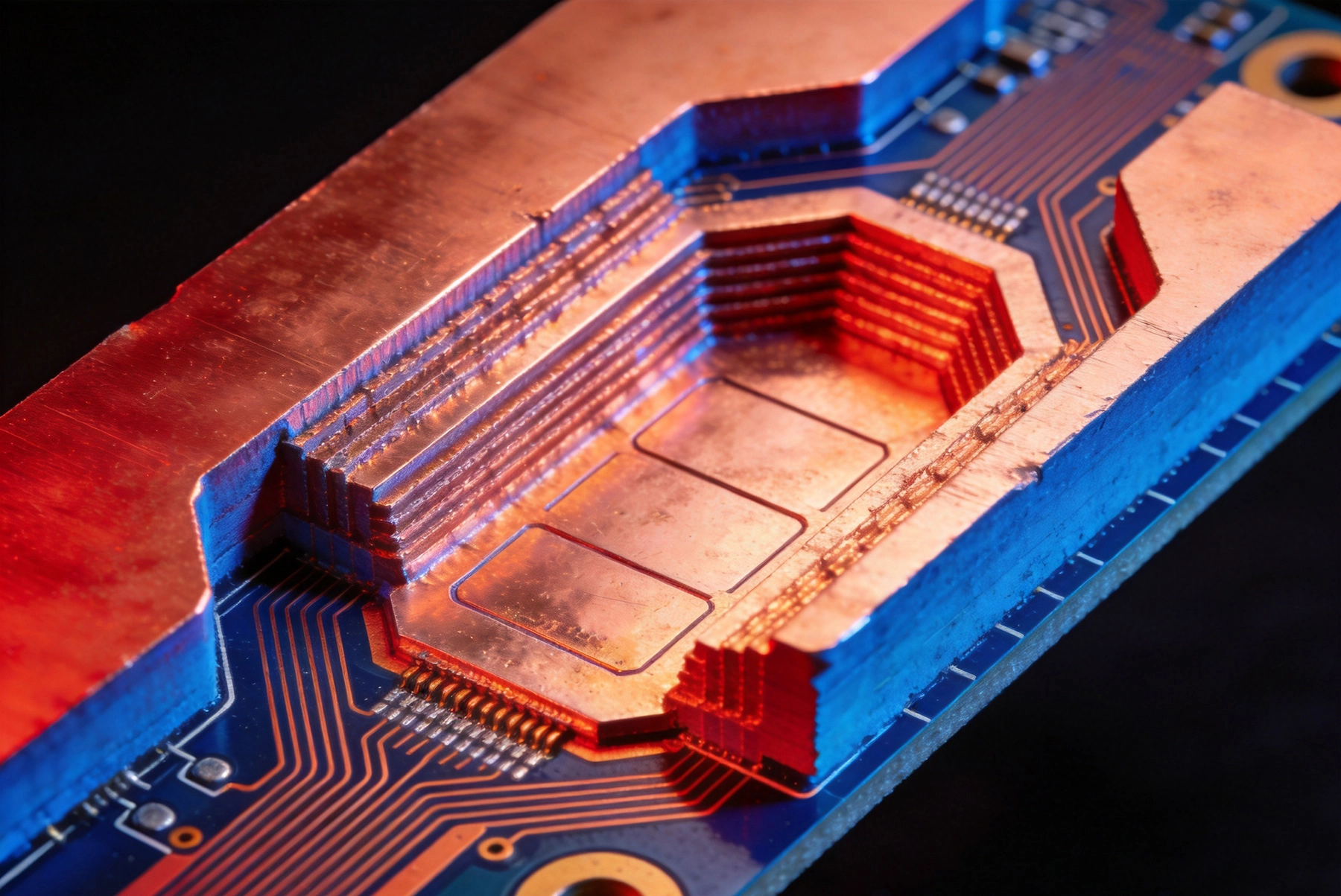
External Heavy Copper refers to thick copper layers on the outer surfaces of the PCB — typically the top and bottom layers. Standard PCB Copper Thickness is 1 oz (35 µm), but heavy copper designs use 2 oz (70 µm), 3 oz (105 µm), 4 oz (140 µm), or even 6-10 oz (210-350 µm) on the outer layers. These thick outer traces and planes carry High Current directly and are exposed to the ambient environment on at least one side.
The key thermal characteristic of external copper is that it has a direct convection path to the surrounding air. The exposed surface can transfer heat through natural or forced convection, and it can also radiate heat to nearby surfaces. This direct thermal coupling to the environment makes external copper inherently efficient at shedding heat — provided there is airflow and space around the board.
Internal embedded copper consists of thick copper planes or shapes buried within the multilayer stack-up, surrounded by dielectric material (prepreg and core laminate). These internal copper features are connected to outer-layer components through Thermal Vias, plated through-holes, or via-in-pad structures. The embedded copper acts as a heat spreader — collecting heat from localized sources and distributing it across a larger area before it reaches the board surface.
The critical difference is that internal copper has no direct convection path. All heat must conduct through the surrounding dielectric material to reach the outer surfaces before it can be transferred to the environment. Since FR4 and similar laminates have relatively low thermal conductivity — typically 0.3-0.4 W/m·K — this conduction path introduces significant Thermal Resistance compared to the direct convection available to external copper.
Convection is the dominant heat transfer mechanism for PCBs in most operating environments. The convection heat transfer coefficient for natural convection in still air is typically 5-25 W/m²·K, and for forced convection with moderate airflow it can reach 25-100 W/m²·K. External copper surfaces participate in convection directly.
Internal embedded copper cannot convect at all. Every watt of heat generated in or conducted to an internal copper plane must first travel through dielectric material to reach an external surface. The Thermal Resistance of this path depends on the dielectric thickness and its thermal conductivity:
The result is that internal copper always has higher total thermal resistance to ambient than external copper at the same location. For the same power dissipation, internal copper will run hotter unless other factors compensate.
Where internal copper excels is in heat spreading. Copper's thermal conductivity is approximately 385 W/m·K — roughly 1,000 times higher than FR4. An internal copper plane acts as a highly efficient thermal highway that rapidly distributes localized heat across its entire area. This spreading effect reduces the peak temperature at hot spots by distributing the thermal load.
Consider a power MOSFET dissipating 5 W on a small pad. Without an internal copper plane, the heat is concentrated in the pad area and must conduct through the local dielectric and copper to reach surrounding traces. With an internal copper plane connected through Thermal Vias, the heat spreads across the entire plane area almost instantaneously (on thermal timescales), reducing the local temperature rise by a factor that depends on the ratio of plane area to source area.
This spreading benefit is most pronounced when:
Radiative heat transfer from PCB surfaces depends on the surface emissivity and the fourth-power temperature difference between the board and surroundings. For typical solder mask surfaces (emissivity ≈ 0.9-0.95), radiation can account for 10-25 percent of total heat transfer in natural convection environments at moderate temperature rises (40-60°C above ambient).
External copper with solder mask coating participates in radiation. Bare copper, with its low emissivity (≈ 0.05-0.1), radiates poorly — but in practice, most external copper on production boards is covered by solder mask. Internal copper does not radiate at all, since it is surrounded by opaque dielectric material.
Thermal vias are the primary mechanism for transferring heat from external component pads to internal copper planes. Their effectiveness depends on several factors:
For designs using internal embedded copper planes, the thermal via array is often the bottleneck in the heat path. A typical 5-via array of 0.3 mm vias with standard plating has a thermal resistance of roughly 15-25°C/W per via, or 3-5°C/W for the array. This may be acceptable for moderate power levels but becomes limiting for high-power devices dissipating 10+ watts.
In practice, the most effective High Current PCB thermal designs use a combination of internal and external copper. The hybrid approach leverages the strengths of each:
A typical hybrid stack-up for a 4-layer power board might look like this:
This configuration gives the power devices three heat paths: direct convection from the top surface, conduction through thermal vias to the internal spreading plane, and conduction through the board to the bottom convection surface. The result is typically 20-40 percent lower junction temperature compared to either internal-only or external-only approaches.
Absolutely, and you should when the design allows it. External heavy copper handles convection and direct component heat extraction, while internal planes spread heat and provide shielding. Just be aware that combining heavy external copper (3+ oz) with internal planes increases the total copper volume in the board, which can affect lamination quality and requires careful Copper Balancing to prevent warpage.
It matters significantly. Halving the dielectric thickness between an internal plane and the outer surface roughly doubles the conduction heat transfer rate through that layer. Going from 0.2 mm to 0.1 mm dielectric can reduce the temperature rise of the internal copper by 15-25 percent. If thermal performance is critical, work with your fabricator to specify thin prepreg layers between the thermal plane and the outer surfaces.
Yes, but the dynamics change. In a sealed enclosure with no airflow, convection is minimal for both internal and external copper. In potting compound, convection is eliminated entirely and replaced by conduction through the potting material. In these environments, the heat spreading function of internal copper becomes the primary benefit, while the convection advantage of external copper is largely lost. The internal plane should be as large as possible to maximize the conduction area to the enclosure walls or potting interface.
Copper coins are solid copper pieces embedded in the PCB substrate, typically directly under a high-power component. They provide an extremely low thermal resistance path — roughly 5-10× better than a thermal via array — because the heat conducts through solid copper rather than through dielectric and via barrels. Copper coins are used in the highest power applications (50+ amps per device) where thermal via arrays cannot provide sufficient heat extraction. They are more expensive to manufacture but are justified when the alternative is component derating or active cooling.
Solder mask has low thermal conductivity (≈ 0.2 W/m·K) and is typically 10-25 µm thick, so it does add a small thermal resistance. However, this resistance is negligible compared to the convection resistance at the surface. The more important effect of solder mask is on radiation: solder mask has high emissivity (0.9+), which improves radiative heat transfer compared to bare copper (emissivity ≈ 0.05). In natural convection environments, solder mask can actually improve overall thermal performance by 5-10 percent due to this radiation benefit.
The choice between internal embedded copper and external heavy copper for Heat Dissipation is not an either-or decision — it is a question of how to combine both for maximum thermal performance. External copper excels at direct convection to the environment, making it the clear choice for exposed traces and pads in airflow. Internal copper excels at heat spreading and EMI shielding, making it essential for distributing concentrated heat loads and protecting signal integrity. The most effective High Current PCB thermal designs use a hybrid approach that leverages the convection advantage of external copper and the spreading advantage of internal planes, connected through well-designed thermal via arrays. By understanding the thermal mechanics of each approach and applying the design guidelines outlined here, you can make informed decisions that keep your power devices within safe operating temperatures without over-designing the board or exceeding your manufacturing budget.
Contact us to discuss your requirements
Cost Comparison: 2oz vs 4oz Copper PCB — What You Need to KnowJune/26/2026
High Current PCB Layer Stackup: Symmetrical vs. Asymmetrical Power PlanesJuly/20/2026
High Current PCB Via Plating: 1mil vs. 2mil Thickness Reliability TestAugust/03/2026
High Current PCB Annular Rings: Minimum Size vs. Reinforced SizeAugust/12/2026
High Current PCB Solder Wicking: Tented Vias vs. Untented ViasSeptember/01/2026
High Current PCB Testing: Thermal Imaging vs. 4-Wire Kelvin MeasurementJuly/22/2026
High Current PCB Current Crowding: Sharp Corners vs. Teardrop TransitionsSeptember/03/2026
High Current PCB Trace Width Calculator: The Ultimate Engineering GuideMay/20/2026