Mounting holes on printed circuit boards serve a dual purpose that many designers overlook: they secure the board to its chassis or enclosure, and when properly designed, they can also serve as critical current return paths between the PCB ground plane and the system chassis ground. For high-power applications where tens or even hundreds of amps flow through ground return paths, the choice between plated and non-plated mounting holes has significant implications for current capacity, thermal performance, electromagnetic compatibility, and long-term reliability. Making the wrong choice can lead to excessive voltage drop in ground paths, overheating at mounting points, Ground Loop problems, and even catastrophic failure of the ground connection. This article examines both options in detail to help you make the right decision for your High Current Design.

Understanding the Two Types of Mounting Holes
Plated Mounting Holes (Plated Through Holes - PTH)
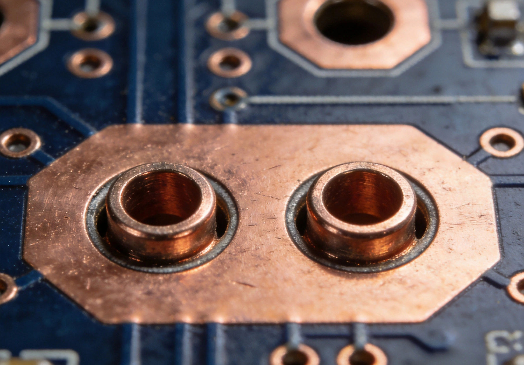
Plated mounting holes have a cylindrical copper plating (the barrel) deposited on the inner wall of the drilled hole, electrically connecting the hole to copper features on every layer of the PCB that the hole passes through. The copper barrel typically has a plating thickness of 20-25μm (0.8-1.0 mil) for standard boards, but can be increased to 35μm or more for high-current applications.
- The copper barrel creates a continuous conductive path from the top copper layer, through any internal layers, to the bottom copper layer
- A copper Annular Ring (pad) surrounds the hole on each connected layer, providing additional copper area for current spreading and solder attachment
- Plated holes can be connected to ground planes, Power Planes, or left as isolated through-connections depending on design requirements
- When connected to a ground plane, the plated hole provides a low-impedance electrical connection between the PCB ground and any conductive mounting hardware
Non-Plated Mounting Holes (NPTH)
Non-plated mounting holes are simply drilled holes through the PCB substrate with no copper plating on the inner wall. They serve exclusively as mechanical mounting features with no electrical connectivity between layers.
- The hole passes through all copper layers without making electrical contact—copper features on each layer are pulled back from the hole edge by a defined clearance
- Non-plated holes are electrically isolated from all copper features on the PCB
- They provide only mechanical fixation with no current-carrying capability
- Any electrical connection to the chassis or enclosure must be established through separate means (dedicated ground vias, edge connectors, or external ground straps)
Current Return Path Fundamentals
In high-Power Electronics, the ground return path is not simply a reference potential—it carries the full operating current of the system. The quality of this return path directly affects circuit performance, electromagnetic emissions, and system reliability.
Why Mounting Holes Matter for Current Return
- Chassis Ground Connection: In many industrial, automotive, and Power Electronics systems, the PCB ground plane must connect to the metal chassis for both electrical safety (protective earth) and electromagnetic shielding. Mounting hardware (screws, standoffs, washers) provides this connection, but only if the mounting holes are designed to conduct current effectively.
- Ground Plane Stitching: Plated mounting holes connected to ground planes act as ground stitching vias, reducing ground plane impedance at the board perimeter and improving high-frequency grounding performance for electromagnetic compatibility.
- Thermal Grounding: The chassis often serves as a heat sink. Plated mounting holes connected to ground planes provide thermal pathways from the PCB to the chassis, supplementing primary Thermal Management and reducing board temperature.
- ESD and Surge Protection: Plated mounting holes connected to chassis ground provide low-impedance discharge paths for electrostatic discharge (ESD) and surge events, protecting sensitive circuitry from transient damage.
Plated Mounting Holes for Current Return: Detailed Analysis
Advantages
- Defined Current Path: The copper barrel provides a well-defined, predictable current path with calculable resistance and current capacity. For a 3.2mm diameter hole with 25μm plating, the cross-sectional area of the copper barrel is approximately 0.25mm², capable of carrying roughly 2-3A continuously.
- Low-Impedance Ground Connection: When connected to ground planes on multiple layers, the plated hole provides a very low-impedance connection (typically less than 1mΩ) between the PCB ground and mounting hardware, minimizing ground voltage drop and noise.
- Multi-Layer Ground Stitching: Plated mounting holes automatically connect all ground planes through the PCB stackup, providing effective ground plane stitching without additional vias. This reduces ground plane resonance and improves EMC performance.
- Solderable Connection: The copper barrel can be soldered to mounting hardware or washers, creating a permanent, low-resistance electrical connection that will not degrade over time due to oxidation or loosening of mechanical fasteners.
- Thermal Transfer: The copper barrel provides an additional thermal conduction path from internal ground planes to the chassis, improving Heat Dissipation for high-power designs.
- ESD and Surge Path: The low-impedance path through the plated hole provides effective discharge routing for electrostatic discharge and surge events to chassis ground.
Limitations and Design Considerations
- Limited Current Capacity per Hole: The thin copper barrel (20-25μm plating) limits the current a single plated mounting hole can carry. For high-current applications exceeding 5-10A per mounting point, the standard plating thickness is insufficient and must be increased, or multiple plated holes must be used in parallel.
- Plating Quality Risks: The copper barrel in mounting holes is subject to cracking or voids during drilling, assembly, or Thermal Cycling, especially in large-diameter holes where the aspect ratio is low. These defects can increase resistance or create open circuits in the ground path.
- Thermomechanical Stress: During Thermal Cycling, the difference in CTE between the copper barrel and the PCB substrate can cause barrel cracking, particularly in larger-diameter holes. This risk increases with the number of thermal cycles and the temperature range.
- Galvanic Corrosion: When dissimilar metals are in contact (copper barrel against steel screws or aluminum chassis), galvanic corrosion can increase contact resistance over time, particularly in humid or corrosive environments. Proper material selection and protective finishes are essential.
- Assembly Stress: Tightening mounting screws applies significant compressive force to the copper barrel and surrounding Annular Ring. Excessive torque can crush the barrel, delaminate the pad, or create micro-cracks that degrade the electrical connection.
Design Best Practices for Plated Mounting Holes
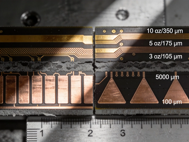
- Increase Plating Thickness: For high-current applications, specify increased copper plating thickness (35-50μm or more) in mounting holes to improve current capacity and mechanical robustness. Many fabricators support heavy plating for mounting holes as a special construction requirement.
- Use Large Annular Rings: Design generous annular rings (pads) around plated mounting holes to provide additional copper area for current spreading, improve solder joint strength, and reduce Current Density at the hole edge. A minimum annular ring of 0.5mm beyond the hole diameter is recommended for high-current applications.
- Connect to Multiple Ground Planes: Connect plated mounting holes to all ground layers in the stackup to maximize current capacity and minimize impedance. Multiple parallel ground connections through different layers share the current and provide redundancy.
- Use Multiple Mounting Holes in Parallel: For very high currents, distribute the return current across multiple plated mounting holes rather than relying on a single hole. Four plated mounting holes in parallel can carry roughly four times the current of a single hole while reducing the Current Density and heating at each point.
- Specify Appropriate Surface Finish: Use surface finishes that maintain solderability and conductivity over the product lifetime. Hot air solder leveling (Hasl), immersion silver, or electrolytic nickel/gold provide good conductivity for ground connections. Avoid finishes that increase contact resistance (OSP, certain Enig formulations with thick nickel barriers).
- Use Washers for Current Spreading: Large-diameter conductive washers (copper or tin-plated brass) between the screw head and the PCB pad spread the current over a larger area, reducing current density and improving the reliability of the electrical connection.
- Control Screw Torque: Specify and control mounting screw torque to ensure consistent contact pressure without overstressing the copper barrel. Too little torque results in high contact resistance; too much torque damages the plating.
Non-Plated Mounting Holes for Current Return: Detailed Analysis
When Non-Plated Holes Are the Right Choice
- Isolated Ground Architecture: When the PCB ground must be electrically isolated from the chassis ground (common in medical equipment, sensitive measurement instruments, and systems requiring isolated grounding), non-plated mounting holes prevent unintended ground connections through the mounting hardware.
- Preventing Ground Loops: In systems where multiple ground connection points through mounting hardware could create ground loops that inject noise into sensitive circuits, non-plated holes allow controlled single-point grounding through a dedicated, designed ground connection.
- Reducing Thermomechanical Stress: Without a copper barrel, non-plated holes eliminate the risk of barrel cracking during thermal cycling, improving mechanical reliability for applications with extreme temperature swings.
- Simplified Manufacturing: Non-plated holes avoid the plating process entirely, reducing manufacturing steps and eliminating plating-related defects. This can improve yield for boards with many large-diameter mounting holes.
- Precision Mechanical Alignment: Non-plated holes can be drilled more precisely after plating (as a secondary drilling operation), providing tighter dimensional tolerances for applications requiring precise board-to-chassis alignment.
Establishing Current Return with Non-Plated Holes
When using non-plated mounting holes, you must provide an alternative means of establishing the Current Return Path to chassis ground:
- Dedicated Ground Pads with Separate Vias: Place copper pads near each mounting hole, connected to the ground plane through multiple heavy-plated vias. Conductive mounting hardware (screws, washers, standoffs) contacts these pads to establish the ground connection, while the mounting hole itself remains non-plated and electrically isolated.
- Edge Card or Board Edge Ground Connections: Use copper features along the board edge that contact conductive chassis rails or frame members when the board is inserted, providing ground connection without relying on mounting holes.
- External Ground Straps or Bus Bars: For very High Current applications, dedicated ground bus bars or heavy-gauge wire straps provide lower resistance and higher current capacity than any through-hole connection, connecting the PCB ground to chassis ground independently of the mounting hardware.
- Connector-Based Grounding: Ground connections through board-to-board or board-to-chassis connectors can provide reliable, controlled-impedance ground paths without relying on mounting hardware.
Comparative Analysis: Plated vs. Non-Plated for High Current
- Current Capacity: Plated holes provide a defined current path but are limited by plating thickness. Non-plated holes require alternative return paths, but these alternatives (bus bars, dedicated ground vias) can often provide higher current capacity than plated mounting holes.
- Connection Reliability: Plated holes rely on the copper barrel and mechanical contact pressure for the electrical connection, both of which can degrade over time. Non-plated approaches using dedicated ground connections can be more reliable as they are not subject to mechanical stress from mounting hardware.
- Design Flexibility: Non-plated holes offer more flexibility in ground architecture, allowing isolated, single-point, or multi-point grounding strategies. Plated holes inherently create multi-point ground connections that may or may not be desired.
- EMC Performance: Plated mounting holes provide ground plane stitching that improves EMC performance by reducing ground plane impedance at the board perimeter. Non-plated holes lose this benefit unless dedicated ground stitching vias are added nearby.
- Thermal Performance: Plated holes provide a thermal path from internal ground planes to the chassis. Non-plated holes require separate Thermal Vias or thermal interface materials for board-to-chassis heat transfer.
- Manufacturing Cost: Non-plated holes are simpler to manufacture, but the additional dedicated ground features (pads, vias, connectors) needed to replace the ground function may offset or exceed this cost advantage.
Application-Specific Recommendations
Industrial Power Electronics (VFDs, Inverters, Power Supplies)
Use plated mounting holes with increased plating thickness (35μm+), large annular rings, and connection to all ground layers. Supplement with multiple parallel mounting holes and conductive washers for current sharing. This application demands maximum current capacity and reliable chassis grounding for safety and EMC.
Automotive Electronics (ECUs, BMS, Inverters)
Use plated mounting holes with heavy plating and robust annular rings connected to ground planes. Automotive environments subject connections to extreme vibration and thermal cycling, making the mechanical robustness of well-designed plated holes preferable. Specify torque requirements for mounting hardware to ensure consistent contact.
Medical and Measurement Equipment
Use non-plated mounting holes to maintain ground isolation between PCB ground and chassis ground. Establish the required ground connection through a single, controlled dedicated ground point to prevent ground loops and maintain measurement accuracy.
Consumer Electronics (Moderate Power)
For moderate-current consumer applications (less than 5A ground current), standard plated mounting holes with default plating thickness provide adequate current capacity and EMC grounding. The cost and complexity of alternative approaches is not justified.
Telecommunications and Data Center Equipment
Use plated mounting holes for EMC grounding and ground plane stitching, but verify that the ground architecture does not create unwanted ground loops that could affect signal integrity in high-speed data paths. Careful placement and selective connection of mounting hole grounds may be required.
Common Design Mistakes to Avoid
- Relying on a Single Plated Mounting Hole for High Current: A single plated mounting hole with standard plating cannot carry more than a few amps safely. Distribute high return currents across multiple parallel paths.
- Ignoring Plating Thickness in Current Calculations: The current capacity of a plated hole depends on the cross-sectional area of the copper barrel, which is determined by both hole diameter and plating thickness. Always calculate current capacity based on actual plating thickness, not just hole diameter.
- Assuming Mounting Hardware Provides Reliable Contact: Mechanical contact between a screw and a plated pad is not inherently reliable. Oxidation, contamination, insufficient torque, and vibration can all increase contact resistance. Soldered connections or spring-loaded hardware provide more reliable contact.
- Mixing Plated and Non-Plated Holes Inconsistently: If some mounting holes are plated and connected to ground while others are non-plated and isolated, verify that the intended ground architecture is actually achieved. Unintended ground connections or missing connections can cause functional or EMC problems.
- Neglecting Thermal Effects on Contact Resistance: Thermal cycling can degrade the contact between mounting hardware and plated pads over time, gradually increasing ground path resistance. Design for long-term reliability by specifying appropriate materials, finishes, and torque values.
Conclusion
The choice between plated and non-plated mounting holes for High Current PCB return paths is not a simple binary decision—it depends on your current requirements, grounding architecture, environmental conditions, and reliability needs. Plated mounting holes provide an integrated, convenient Current Return Path through the copper barrel but are limited by plating thickness and subject to mechanical degradation. Non-plated mounting holes offer design flexibility and eliminate plating-related failure modes but require alternative ground connections that add complexity and cost. For most high-power industrial and automotive applications, well-designed plated mounting holes with increased plating thickness, generous annular rings, and proper mounting hardware provide the best combination of current capacity, EMC performance, and convenience. For applications requiring ground isolation or where plating reliability is a concern, non-plated holes with dedicated ground connections offer a more appropriate solution.
Contact us to discuss your requirements.