

Electronic Speed Controllers governing drone motors face some of the most demanding Pcb Design challenges in consumer electronics. These compact controllers must switch hundreds of amperes at tens of kilohertz while maintaining efficiency above 95 percent and fitting within the strict size constraints of modern drone frames. The key to achieving this performance lies in understanding how loop inductance affects switching losses, voltage spikes, and overall efficiency. Engineers who master the art of minimizing loop inductance in high-current ESC designs create controllers that run cooler, last longer, and deliver the responsive throttle control that drone pilots depend on.
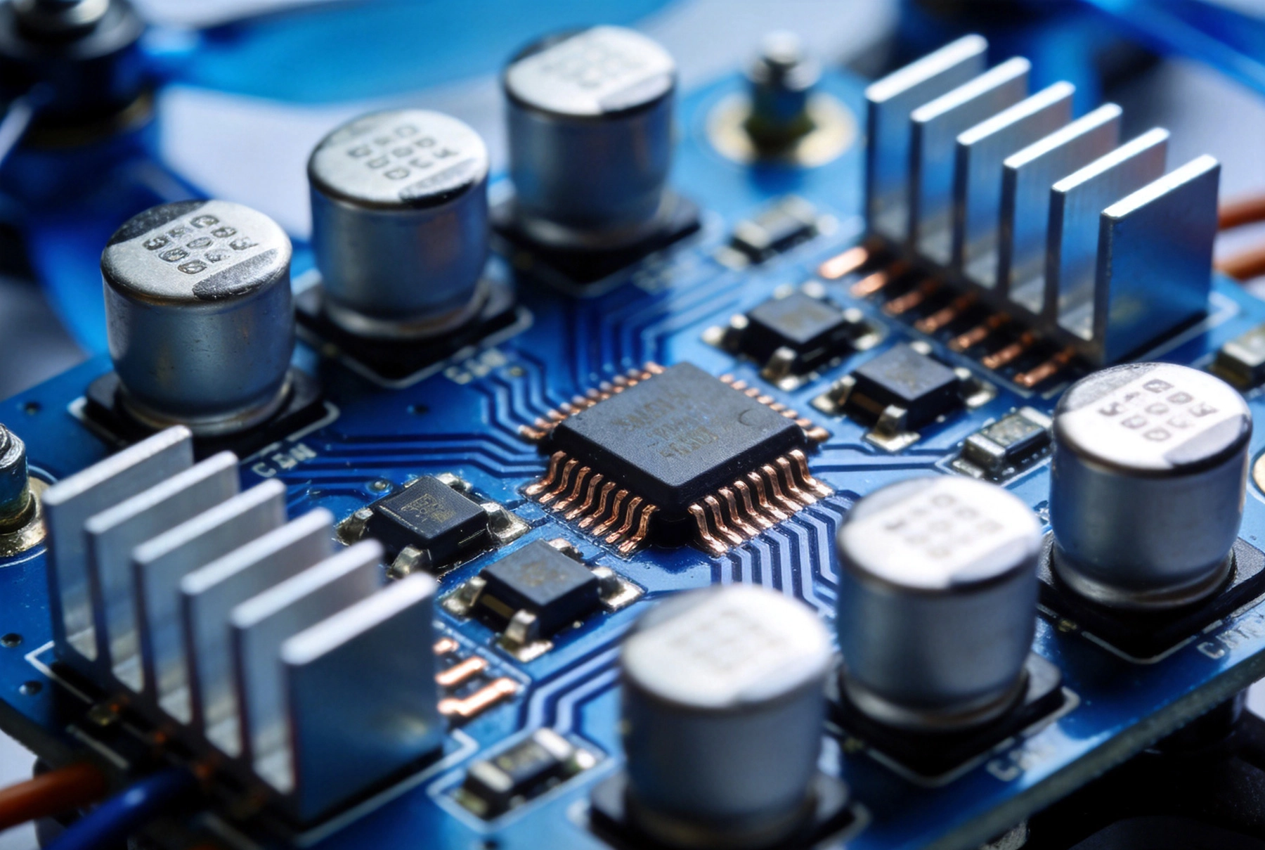
Every current loop in a power switching circuit stores energy in its magnetic field. This stored energy, measured in nanohenries for typical PCB loops, manifests as voltage spikes when the current tries to change abruptly. For drone ESCs switching at 20 to 40 kilohertz, the rate of current change reaches thousands of amperes per microsecond. At these slew rates, even small loop inductances create voltage transients that stress semiconductor devices and reduce efficiency.
The loop inductance of a Pcb Trace depends on its geometry. Wider traces closer to ground planes have lower inductance than narrow traces suspended above dielectrics. The distance between the power and return paths matters most—a loop with traces separated by 1 millimeter has roughly ten times the inductance of the same loop with traces separated by 0.1 millimeters. This geometric sensitivity explains why ESC layout directly determines electrical performance.
When MOSFETs switch in drone ESC applications, they experience voltage stress equal to the supply voltage plus the inductive spike. A 6S lithium-polymer battery providing 25 volts creates nominal stress, but inductive spikes can push peak voltages to 35 or 40 volts. Devices rated at 30 volts may fail prematurely when subjected to repeated transients beyond their specifications. Minimizing loop inductance directly extends component lifetime.
Modern drone ESCs use a three-phase bridge configuration with six MOSFETs to drive the three motor windings. Each half-bridge consists of a high-side and low-side MOSFET that alternate conduction to generate the three-phase outputs. The power loop for each half-bridge includes the input capacitors, the two MOSFETs, and the motor winding connecting to the next phase. These three power loops must each be optimized for minimum inductance.
The physical arrangement of MOSFETs significantly affects loop inductance. Placing the high-side and low-side MOSFETs on opposite sides of the PCB forces current to travel around the board perimeter, creating larger loops. A more compact arrangement with MOSFETs adjacent to each other, oriented to create current flow in opposite directions, can reduce loop area by 80 percent compared to spread-out layouts.
The input capacitors serve two critical functions: providing bulk energy storage for peak current demands and filtering high-frequency current transients that would otherwise propagate through the battery wiring. Drone ESCs typically use a combination of electrolytic bulk capacitors for energy storage and ceramic capacitors for high-frequency filtering. The ceramics positioned closest to the MOSFET switching nodes directly affect loop inductance.
Ceramic capacitor placement determines their effectiveness. When placed centimeters away from the MOSFETs, ceramic capacitors become part of longer loops that provide little high-frequency decoupling. The capacitors must be within millimeters of the MOSFET source and drain pins to effectively short high-frequency transients. This proximity requirement conflicts with the need to route motor phase connections, requiring careful layout optimization.
Modern drone ESC designs increasingly use DirectFET or similar MOSFET packages with metal slugs for top-side heat extraction. These packages also offer significant advantages for loop inductance because the source and drain connections span the package width, providing broad current paths that reduce effective series resistance. The flat, wide geometry of these packages creates inductances 30 to 50 percent lower than comparable SO-8 packages.
The drain and source connections on DirectFET packages enable a layout technique called Kelvin source sensing. A separate, physically small connection to the source pin carries the gate drive return current, while the main source connection handles high-current return. This separation prevents the high di/dt currents from inducing voltage drops in the gate drive loop, which would slow switching transitions and increase switching losses.
The routing between input capacitors and MOSFETs must minimize loop area while accommodating the physical dimensions of components. A technique called cross-under or overlay routing places the power and ground planes on adjacent layers directly below the switching node, with the capacitor pads and MOSFET pads connected through Thermal Vias. This approach creates a compact loop that threads through the PCB rather than spreading across its surface.
For the motor phase outputs, routing must balance loop inductance against the need to dissipate heat generated in the MOSFETs. Phase traces that spread heat across larger copper areas also spread loop inductance across those same areas. Optimizing the phase routing requires simulation and measurement to find the geometry that best trades these competing requirements.
Ground planes directly beneath high-current loops provide return paths that minimize effective loop area. When current flows in the power trace, equal current returns in the ground plane directly below, creating a transmission line structure with very low loop area. However, slots, splits, or missing copper in the ground plane打断 this return path and force current to find alternative routes that greatly increase loop area.
Drone ESC layouts must avoid ground plane slots beneath the power stage. Motor phase connections often require routing between phases, but these routes should not create slots extending under the switching loops. If phase routing absolutely requires breaking the ground plane, the break should occur perpendicular to the current flow rather than parallel, minimizing the increase in return path length.
Drone ESCs typically operate at 95 to 98 percent efficiency, which means 2 to 5 percent of the controlled power appears as heat in the controller. For a 100-watt ESC controlling a motor running at full throttle, 3 watts of heat must somehow leave the controller. In compact racing drone ESCs where the controller must fit within 30 by 30 millimeters, this heat flux approaches values found in server power supplies.
The heat generated in MOSFETs during switching consists of both conduction losses and switching losses. Conduction losses depend on the MOSFET on-resistance and the RMS current flowing through the device. Switching losses depend on how quickly the device transitions between on and off states, which in turn depends on gate drive current and the voltage and current being switched. Optimizing for low switching losses requires fast transitions, while optimizing for low conduction losses requires low on-resistance. The optimal device balances these competing requirements.
The PCB itself becomes the primary Heat Dissipation path for most drone ESCs. Copper planes spreading heat from the MOSFETs to the motor connectors and battery wiring provide thermal conduction to the ambient air. Increasing Copper Weight from the standard 1-ounce to 2-ounce or 3-ounce construction significantly improves thermal spreading, though it increases cost and complicates plating for vias.
Thermal Vias connecting the MOSFET drain pads to underlying ground planes carry heat away from the switching devices. These vias should be numerous, small in diameter, and placed directly under the device to minimize Thermal Resistance. The copper plating inside the vias provides thermal conductivity comparable to solid copper, making well-designed via arrays effective at removing heat from surface-mounted components.
Racing drones typically fly at high speeds that provide significant forced-air cooling for ESCs mounted on the frame. The airflow over the ESC removes heat from the PCB surface through convection. Designing the PCB with large surface area exposed to airflow helps this cooling mechanism, though it conflicts with the enclosed, protected mounting positions that protect electronics during crashes.
Some ESC designs incorporate dedicated heatsinks that attach to the MOSFETs or the PCB surface. These heatsinks add weight and complexity but can significantly extend the continuous power rating of a controller. When evaluating ESCs for racing applications, the presence of adequate heatsinking often distinguishes controllers rated for burst power from those capable of continuous high-power operation.
The gate resistor controls the rate at which charge enters or leaves the MOSFET gate during switching transitions. Smaller resistors provide faster switching and lower switching losses, but can cause ringing and electromagnetic interference. Larger resistors slow transitions and increase switching losses, but damp oscillations that could otherwise cause false triggering. The optimal gate resistance balances these considerations for each specific MOSFET and layout.
For drone ESCs with MOSFETs switching hundreds of amperes, the switching speed directly affects efficiency. Faster transitions mean less time spent in the high-loss region where both voltage and current are significant. However, the extremely high di/dt during fast transitions excites the resonant circuits formed by loop inductance and MOSFET capacitances, potentially causing voltage overshoot beyond safe limits. Gate resistance selection requires matching to the specific loop inductance of the layout.
Drone ESC three-phase bridges require floating gate drive circuits for the high-side MOSFETs that switch the motor phase outputs relative to the battery positive rather than ground. The bootstrap circuit uses a capacitor charged through a diode from the low-side supply to provide the gate drive voltage for high-side switching. This approach works well at lower frequencies but introduces timing delays that affect pulse-width modulation accuracy at the high switching frequencies used in modern ESCs.
Modern ESC designs increasingly use specialized gate drive ICs that incorporate desaturation detection and soft turn-off features. These protections detect when MOSFETs experience overcurrent conditions and gracefully turn off the device rather than allowing destructive thermal runaway. The desaturation detection timing must account for the voltage rise caused by loop inductance, preventing false triggers during normal switching transients.
The physical arrangement of components on the ESC PCB determines what routing options remain available. Input capacitors must be as close as possible to the MOSFETs to minimize the critical high-frequency loop. MOSFETs should be arranged to allow short, wide traces for both power and gate drive connections. The motor output connectors should be positioned to allow thick traces from the phase nodes without creating long detours around other components.
Gate drive components including the driver IC and associated resistors and diodes should be positioned between the driver IC and the MOSFET gates. These small components do not consume board area for power dissipation, so they can be placed without regard for thermal considerations. However, their placement affects gate loop inductance, which influences switching speed and EMI characteristics.
Drone ESCs push the limits of standard PCB Fabrication capabilities. The fine pitch between MOSFET pins requires careful solder mask design and accurate registration. The High Current traces demand adequate Copper Weight and plating quality for plated-through holes and vias. Thermal Management requirements may justify Heavy Copper construction with 2-ounce or 3-ounce copper on power layers.
When designing ESCs for manufacturing, consider the tolerances of standard fabrication processes. Minimum line widths and spacings should respect standard capabilities rather than requiring special handling. Via sizes should be producible with standard drill equipment. These considerations ensure that the design translates from prototype to production without requiring expensive or unreliable manufacturing processes.
Thermal imaging during operation reveals hot spots that indicate areas of concentrated dissipation. An ideal ESC shows relatively uniform temperature distribution across the power stage, indicating effective thermal spreading. Hot spots near specific MOSFETs may indicate poor thermal connection to the PCB or imbalanced current sharing between paralleled devices.
Thermal testing should cover the full operating range, from minimum throttle where dissipation is low to full throttle where dissipation peaks. The transient thermal response during sudden throttle changes reveals how effectively the thermal mass of the PCB and components absorbs short-term heat input before reaching equilibrium temperature.
Efficiency measurement across the full throttle range reveals how well the ESC design minimizes switching and conduction losses. Peak efficiency typically occurs near 50 percent throttle where switching losses are balanced against conduction losses. Efficiency degradation at high throttle indicates conduction losses dominating, while efficiency degradation at low throttle suggests switching losses becoming significant relative to the lower average current.
Comparing efficiency measurements between different layouts or component selections quantifies the benefits of specific design choices. A 0.5 percent improvement in efficiency may seem modest but represents 10 percent reduction in heat generation for a controller operating at 95 percent efficiency. These improvements compound over the operating life of the ESC.
What is an acceptable loop inductance target for drone ESC designs?
Modern high-performance drone ESCs should target loop inductances below 5 nanohenries for the primary switching loop. Designs achieving this target can switch at frequencies above 30 kHz with acceptable switching losses. Achieving sub-5nH loops typically requires DirectFET or similar packages, ceramic capacitors within millimeters of the MOSFETs, and power/ground planes on adjacent PCB layers.
How do I measure loop inductance in my ESC design?
Loop inductance can be measured using an impedance analyzer or network analyzer to measure the impedance of the power loop at frequencies above the self-resonance of the input capacitors. The measured impedance divided by 2πf gives the effective series inductance. Alternatively, measuring voltage transients during switching and dividing by the rate of current change provides the loop inductance directly.
What causes voltage spikes during MOSFET switching?
Voltage spikes result from the relationship V = L × di/dt, where L is the loop inductance and di/dt is the rate of current change during switching. Faster transitions produce larger di/dt, which multiplies by loop inductance to produce larger voltage spikes. The spike magnitude adds to the steady-state voltage across the MOSFET, potentially exceeding ratings.
Should I use silicon or silicon carbide MOSFETs for drone ESCs?
Silicon carbide MOSFETs offer lower switching losses and higher temperature capability than silicon devices, but cost significantly more and require different gate drive voltages. For high-power racing drones where efficiency and power density matter most, SiC MOSFETs provide advantages. For cost-sensitive recreational drones, silicon MOSFETs in modern packages like DirectFET provide adequate performance at lower cost.
How does switching frequency affect ESC efficiency?
Higher switching frequencies enable smaller filtering components and more precise throttle control but increase switching losses that reduce efficiency. The optimal switching frequency balances these considerations based on the specific MOSFET characteristics and thermal constraints. Most modern ESCs operate between 20 and 40 kHz, above the audible range while maintaining reasonable efficiency.
High-current Pcb Design for drone electronic speed controllers requires careful attention to loop inductance at every stage of the design process. From component selection through layout optimization to Thermal Management, each decision influences how effectively the ESC controls motor power with minimal losses. The techniques described in this article—compact MOSFET placement, adjacent power and ground planes, optimized capacitor positioning, and appropriate gate drive design—work together to minimize the parasitic inductances that limit switching performance.
Testing and validation complete the design process by confirming that the layout achieves its intended performance. Thermal imaging reveals hot spots that might indicate Thermal Design weaknesses. Efficiency measurements confirm that switching and conduction losses meet targets across the operating range. These measurements guide design iterations that refine the layout until the ESC delivers the performance demanded by modern drone applications.
The competitive drone market rewards designs that achieve higher efficiency in smaller packages. As motor powers continue increasing and frame sizes continue shrinking, ESC designs must become even more efficient and compact. Engineers who master the fundamentals of loop inductance minimization position themselves to create the next generation of high-performance drone controllers that push the boundaries of what is possible in aerial robotics.
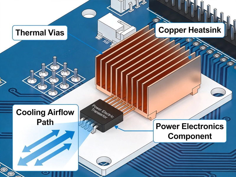
Why Your High-Power PCBs Overheat (And the 5 Methods That Actually Fix It)May/20/2026
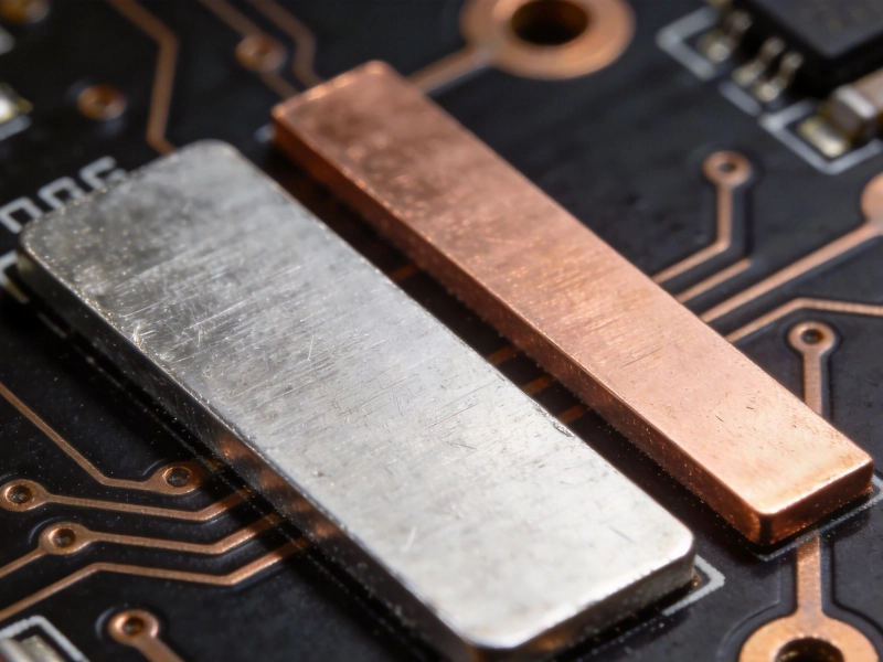
High Current PCB Pad Design: Reinforced Plating vs. Standard PadsJuly/28/2026
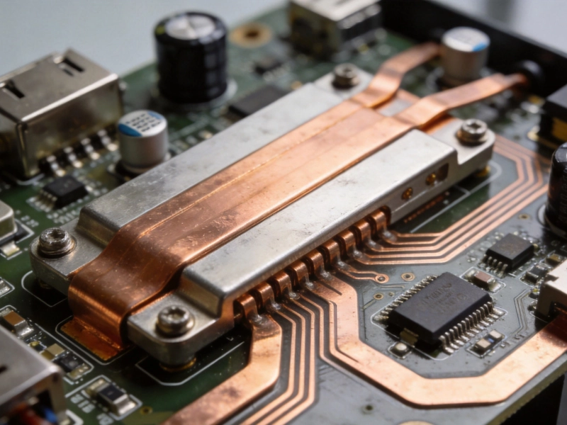
High Current PCB Design for Electric Vehicle Charging StationsAugust/15/2026
A Deep Dive into High Current PCB Design for Solar InvertersJuly/17/2026

High Current PCB Design for Railway Traction SystemsAugust/07/2026
Mastering IPC-2152 Current Carrying Capacity Calculation for Reliable PCB DesignJune/04/2026
High Current PCB Design GuidelinesMay/21/2026

Designing a High Current PCB for Industrial Welding EquipmentJuly/23/2026