

In high-current Pcb Design, every detail matters when it comes to ensuring reliability and performance. The annular ring, the copper pad surrounding a Plated Through-hole, plays a critical role in both electrical connectivity and mechanical integrity. For low-current applications, standard annular ring specifications work adequately. However, when designing PCBs for high-current applications such as power supplies, motor controls, or Led Drivers, the annular ring becomes a crucial design element that requires careful consideration.
The annular ring must reliably carry current from the component lead or wire to the plated barrel of the through-hole. In low-current circuits, this current transfer happens with minimal stress on the copper structure. But at higher current levels, the annular ring experiences significant thermal and mechanical stress that can lead to failure if not properly designed. Understanding the difference between minimum and reinforced annular rings helps engineers make informed decisions that balance performance requirements with manufacturing constraints and cost considerations.
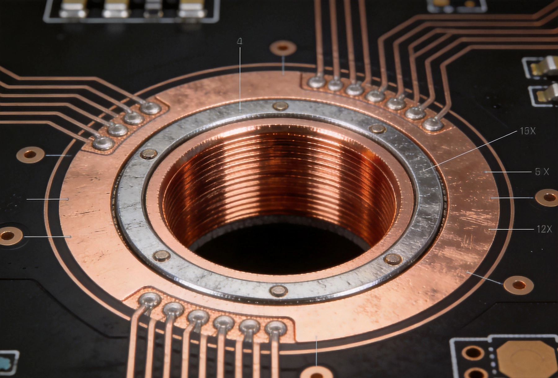
An annular ring is the copper ring or pad that surrounds a Plated Through-hole, connecting the surface pad to the plated barrel that extends through the PCB. When you look at a completed PCB, you see copper pads on the surface with holes drilled through their centers. The annular ring is the copper between the edge of the hole and the outer edge of the pad. This ring serves as the critical interface between surface components and the internal copper layers connected through the barrel plating.
The dimensions of an annular ring are defined by two measurements: the outer diameter of the pad and the diameter of the drilled hole. The annular ring width is calculated as half the difference between these diameters. For example, if a pad has an outer diameter of 1.0mm and the hole is drilled at 0.6mm, the annular ring width would be 0.2mm. This ring must be wide enough to ensure reliable electrical connection and adequate plating coverage while also providing mechanical strength to withstand thermal and mechanical stresses during assembly and operation.
In high-current applications, the annular ring serves additional critical functions beyond simple connectivity. It must dissipate heat generated by current flow through the barrel, provide sufficient cross-sectional area for current to travel from the surface to the barrel, and maintain structural integrity despite Thermal Cycling that occurs during soldering and operation. These requirements often necessitate larger annular rings than would be specified for low-current designs.
Understanding the structure of a plated through-hole helps explain why annular ring design is so important. The hole itself is drilled through the PCB substrate, then electroless and electroplated copper is applied to create the barrel that lines the hole walls. This barrel connects to the copper pads on each surface layer and may connect to internal copper planes in multilayer boards. The annular ring on each surface provides the transition zone between the barrel and the surface pad.
The barrel plating must achieve a minimum thickness specification, typically 20-25 microns for standard applications, to ensure reliable connectivity and adequate current-carrying capacity. However, the barrel itself has limited surface area for Heat Dissipation. The annular ring helps by spreading thermal energy from the barrel to the larger copper pad area, where it can more easily dissipate into the surrounding environment. In high-current designs, this thermal spreading function becomes critical for preventing localized overheating.
The copper structure within the barrel and annular ring forms a continuous metallurgical connection during the plating process. This connection must withstand thermal stresses from soldering operations and from the heat generated during operation. Manufacturing defects such as voids, cracks, or poor adhesion in the annular ring area can lead to premature failures, making process control and quality assurance essential for high-current applications.
Minimum annular ring specifications represent the smallest acceptable ring width that most PCB manufacturers can reliably produce while maintaining functional holes and pads. These specifications typically range from 0.1mm to 0.2mm for standard commercial PCBs, though tighter tolerances may be achievable with premium manufacturing services. The minimum specification exists as a practical limit determined by drilling accuracy, plating process capabilities, and the mechanical integrity of the finished product.
IPC standards define annular ring requirements based on the technology level of the PCB. Class 2 products (standard commercial) typically allow annular rings as small as 0.05mm under certain conditions, while Class 3 products (high-reliability) usually require minimum rings of 0.15mm or larger. These specifications ensure that finished boards meet minimum functionality requirements across normal manufacturing variation. However, meeting these minimums does not mean they represent optimal design choices for high-current applications.
The challenge with minimum annular ring specifications is that they do not account for the specific electrical and thermal requirements of high-current designs. A manufacturer can produce a board with 0.1mm annular rings that passes all inspection criteria but may still fail prematurely in high-current applications due to thermal stress or Current Density limitations. Designers must recognize that meeting minimum specifications and designing for reliability are different objectives requiring different approaches.
Using minimum-size annular rings in high-current applications creates several potential failure mechanisms. The most immediate concern is excessive Current Density. Current flowing from the surface pad into the barrel must pass through the annular ring area, creating a current concentration that increases with decreasing ring width. At sufficiently high currents, this concentration can lead to localized heating that accelerates electromigration and eventually causes failure.
Thermal Cycling represents another significant challenge for minimum annular rings. During operation, the PCB and components generate heat that causes expansion. The copper, substrate, and component leads all have different coefficients of thermal expansion, creating stress at the annular ring interface. Larger annular rings provide more material to absorb this stress and distribute it over a larger area, reducing the likelihood of fatigue-related failures that can occur with smaller rings.
Manufacturing tolerances compound the challenges of minimum annular rings. The drill position, pad registration, and plating variations all contribute to the final annular ring dimensions. A design targeting 0.1mm minimum rings might actually produce some rings as small as 0.05mm due to combined manufacturing variations. For high-current applications, this variation could push some holes below the threshold for reliable operation, creating inconsistent Field Reliability that is difficult to diagnose and correct.
Reinforced annular rings provide enhanced performance for high-current applications by increasing the copper area available for current transfer and thermal dissipation. These larger rings are achieved through wider pads relative to hole diameter, and sometimes through additional copper plating that builds up the ring thickness. The increased dimensions directly address the failure mechanisms that affect minimum-specification rings in high-stress applications.
The primary benefit of reinforced annular rings is reduced current density. Current flowing through the ring experiences lower density in a wider ring because the same current spreads over more copper area. This reduction in current density directly translates to lower temperatures and less stress on the copper structure. For high-current applications, even modest increases in ring width can significantly reduce peak temperatures during operation.
Reinforced annular rings also provide greater mechanical robustness for handling thermal cycling. The larger copper area creates a more substantial connection between the barrel and surface pad, better able to withstand the stresses from differential thermal expansion. This improved mechanical integrity translates directly to longer expected lifespan under thermal cycling conditions, particularly important for applications that see frequent power cycling or operation in variable temperature environments.
Designing reinforced annular rings requires balancing performance requirements against space constraints and manufacturing capabilities. As a practical guideline, targeting annular rings of 0.4mm to 0.6mm width provides significant improvement over minimum specifications while remaining achievable with standard manufacturing processes. Rings wider than 0.6mm offer diminishing returns and may unnecessarily consume board space.
The relationship between pad diameter and hole diameter determines the final annular ring width. For a given hole size, wider rings require larger pads. This trade-off must be considered in the context of overall board density requirements. High-current designs may justify the use of larger pads and wider spacing to accommodate reinforced annular rings, particularly for critical connections such as power inputs, ground returns, and high-current switching nodes.
Pad size requirements for reinforced annular rings should be documented clearly in manufacturing notes and design files. Standard pad sizes built into CAD libraries may not provide adequate ring widths for high-current applications. Creating custom pad stacks optimized for high-current use ensures that manufacturing files include the correct specifications without relying on default library values that may be inappropriate for power applications.
The current-carrying capacity of an annular ring depends on its cross-sectional area and thermal environment. Current must flow from the component lead or surface pad through the annular ring area into the barrel plating. The limiting factor is typically the temperature rise in the ring area, which is influenced by power dissipation, heat transfer to surrounding materials, and the thermal properties of the PCB substrate.
For high-current applications, calculating the current density in the annular ring helps determine the appropriate ring dimensions. Current density is simply the current divided by the cross-sectional area through which it flows. In the annular ring, this is approximately the ring width times the plating thickness. Doubling the ring width halves the current density, directly reducing the temperature rise for the same current level.
Thermal simulation and empirical testing help validate annular ring designs for specific current levels. While theoretical calculations provide starting points, the actual performance depends on many factors including the PCB material, surrounding copper coverage, airflow, and Component Placement. Designs for critical high-current paths should undergo thermal validation to ensure that annular ring temperatures remain within acceptable limits under worst-case operating conditions.
Heat generation in the annular ring area occurs due to the electrical resistance of the copper structure. While the resistance of the annular ring itself is typically small, it is not negligible at High Current levels. The power dissipated in the ring (I²R) converts to heat that must flow away through the pad, barrel, and surrounding materials. If this heat generation exceeds the thermal conductivity of the surrounding structure, temperatures rise and reliability suffers.
Thermal relief spokes connecting the annular ring to surrounding copper planes create additional current paths that help distribute heat generation. However, these spokes also introduce additional resistance and can actually concentrate current into smaller cross-sections if not properly designed. In high-current applications, Thermal Relief Patterns require careful consideration to ensure they provide net benefit rather than creating new bottlenecks.
The PCB material properties significantly influence thermal performance. High-Tg materials typically have better thermal stability but may have lower thermal conductivity. Metal-core PCBs offer dramatically improved thermal conductivity but introduce different design constraints. For extremely high-current applications, the choice of PCB substrate may be as important as annular ring dimensions in achieving reliable thermal performance.
Producing PCBs with reinforced annular rings requires attention to manufacturing capabilities and process controls. Not all PCB manufacturers can reliably produce the larger rings required for high-current applications, particularly when combined with fine-pitch requirements elsewhere on the board. Clear communication of requirements through manufacturing notes and design specifications helps ensure that the chosen manufacturer can meet the necessary tolerances.
Drilling accuracy becomes more critical with reinforced annular rings, though in a counterintuitive way. While tighter drilling tolerances help maintain minimum annular rings, larger rings provide more manufacturing margin for the same positional accuracy. A 0.1mm annular ring design is much more sensitive to drill position variation than a 0.5mm design, making reinforced rings more manufacturable in practice even though they require larger pad sizes.
Plating quality control is essential for high-current annular rings. The copper plating must achieve uniform thickness throughout the barrel and across the annular ring area without voids or discontinuities. Manufacturers should provide statistical process control data showing plating thickness consistency. For critical applications, additional testing such as cross-section analysis or thermal cycling validation may be appropriate to verify plating quality.
Reinforced annular rings generally increase PCB cost through increased material usage and potentially more restrictive manufacturing requirements. Larger pads consume more board area, which may require larger board sizes or reduce the number of boards per panel. These factors directly impact material costs and should be factored into the overall project budget from the beginning.
The manufacturing process for reinforced annular rings is fundamentally similar to standard production, so the incremental cost premium is typically modest compared to the overall cost of specialized materials or processes. Most manufacturers can produce wider pads without significant process changes, making reinforced annular rings a relatively cost-effective way to improve reliability compared to more exotic solutions like heavier copper or metal-core substrates.
When evaluating cost versus benefit, consider the total cost of field failures, warranty claims, and reputation damage that could result from inadequate annular ring design. For products where reliability is critical, the relatively small cost of reinforced annular rings often provides excellent return on investment. This is particularly true for industrial, automotive, or medical applications where failure consequences are severe.
Establish clear annular ring specifications based on actual current requirements rather than default library values. For power connections carrying more than a few amps, specify minimum annular ring widths of 0.4mm or greater. Document these requirements explicitly in your design files and manufacturing notes to ensure they are not lost or overridden by default settings during the release process.
Use thermal simulation or analysis to validate annular ring designs for high-current paths. While rules of thumb provide starting points, actual thermal performance depends on many factors specific to your design. Identifying thermal hotspots before manufacturing allows design optimization that might not be possible after boards are fabricated. Many Pcb Design tools include Thermal Analysis capabilities that can provide valuable insights.
Consider the interaction between annular ring design and other design elements. Surrounding copper coverage affects Heat Dissipation. Via placement can either help by providing additional thermal paths or hurt by removing copper area. Component Placement influences airflow and heat distribution. Optimizing the entire thermal environment around high-current connections often provides better results than focusing solely on annular ring dimensions.
Clearly communicate annular ring requirements to your PCB manufacturer through multiple channels. Design files should include explicit specifications for pad sizes and annular ring requirements. Manufacturing notes should highlight critical high-current connections and explain why enhanced specifications are required. Finally, consider direct communication with the manufacturer's engineering team for complex or critical designs.
Include annular ring verification in your incoming inspection process. Simple visual inspection may not reveal annular ring problems that exist below the surface. Cross-section analysis of prototype boards provides definitive verification of plating quality and ring dimensions. This inspection is particularly important for first articles from new manufacturers or when significant design changes have been implemented.
Document design rationale for annular ring specifications so that future revisions maintain appropriate requirements. Engineers who inherit designs may not understand why non-standard pad sizes were used. Including brief explanations in design documentation ensures that cost-reduction efforts in future revisions do not inadvertently compromise reliability by shrinking annular rings below safe limits.
One common mistake is assuming that meeting minimum manufacturing specifications ensures adequate performance in high-current applications. Minimum annular rings are designed for general-purpose use where current density is not a concern. Applying these specifications to high-current designs without analysis creates reliability risks that may not become apparent until field deployment exposes the inadequacy.
Another frequent error is using different annular ring sizes inconsistently across similar high-current connections. This inconsistency complicates manufacturing and inspection while potentially creating reliability variations between connections. Establish a standard pad size for each hole diameter used in high-current applications and apply it consistently throughout the design.
Neglecting thermal relief design for connections to copper planes represents another common oversight. While thermal reliefs are essential for ensuring solderability during assembly, improper relief designs can actually increase current density in the annular ring by forcing current through narrow spokes. Balance the need for thermal relief against the requirement for adequate current-carrying cross-section.
Q: What is the minimum recommended annular ring width for High-current Pcb applications?
A: For high-current applications (typically above 3-5A), annular ring widths of at least 0.4mm to 0.6mm are recommended. This provides adequate current-carrying capacity and thermal dissipation while remaining achievable with standard manufacturing processes. For extremely high currents or demanding thermal environments, even wider rings may be beneficial.
Q: Can I use larger pads without changing hole sizes to increase annular ring width?
A: Yes, increasing pad diameter while maintaining the same hole size directly increases annular ring width. This is the standard approach for reinforced rings in high-current designs. The trade-off is increased board space consumption, which must be balanced against the performance benefits.
Q: Do reinforced annular rings require special manufacturing processes?
A: Generally no, reinforced annular rings can be produced using standard Pcb Manufacturing processes. The larger pad sizes required are typically easier to manufacture consistently than minimum-specification rings. However, quality control for plating thickness becomes more important to ensure adequate current-carrying capacity.
Q: How do I verify annular ring quality in finished PCBs?
A: Visual inspection can verify ring presence and uniformity but cannot reveal internal defects. Cross-section analysis provides definitive verification of plating quality and actual ring dimensions. For critical applications, thermal cycling testing can identify designs that may be susceptible to fatigue failures over time.
Q: Should I use heavier copper plating for high-current annular rings?
A: Heavy Copper plating (2oz or more) can complement reinforced annular rings for very high-current applications. However, heavier plating may affect the ability to produce fine features elsewhere on the board. Evaluate whether Heavy Copper is necessary for your specific current levels or whether wider rings with standard plating provide adequate performance.
Annular ring design represents a critical but often overlooked aspect of High-current Pcb development. The difference between minimum-specification rings and reinforced rings can determine whether a product operates reliably for years or fails prematurely due to thermal stress or current density issues. Understanding the physics of current flow and heat dissipation in through-hole structures enables informed design decisions that balance performance, cost, and manufacturability.
For high-current Led Drivers, power supplies, motor controls, and similar applications, the marginal cost of reinforced annular rings is a small investment compared to the potential consequences of field failures. Establishing clear design standards for annular ring dimensions, documenting requirements clearly, and verifying compliance through appropriate inspection processes creates a foundation for reliable high-current PCB designs.
As power levels continue to increase in response to demands for higher performance LED lighting, more powerful electronics, and greater energy efficiency, the importance of proper annular ring design will only grow. Engineers who master these design principles today will be well-positioned to address the more demanding applications of tomorrow, creating products that perform reliably in increasingly challenging electrical and thermal environments.
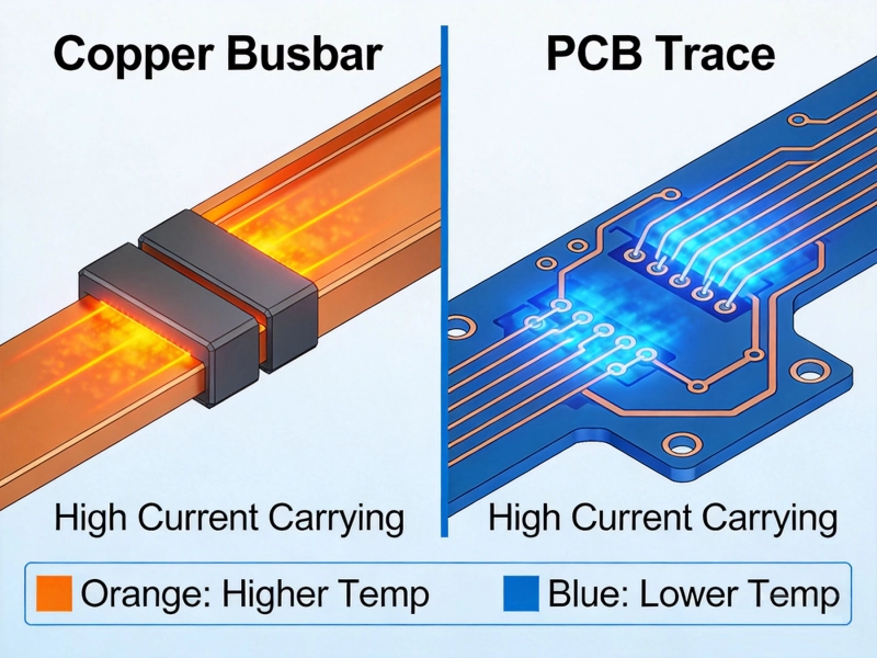
Bus Bar vs PCB Trace for High CurrentMay/21/2026

High Current PCB Bus Bars vs. Heavy Copper Traces: Cost and PerformanceJuly/25/2026
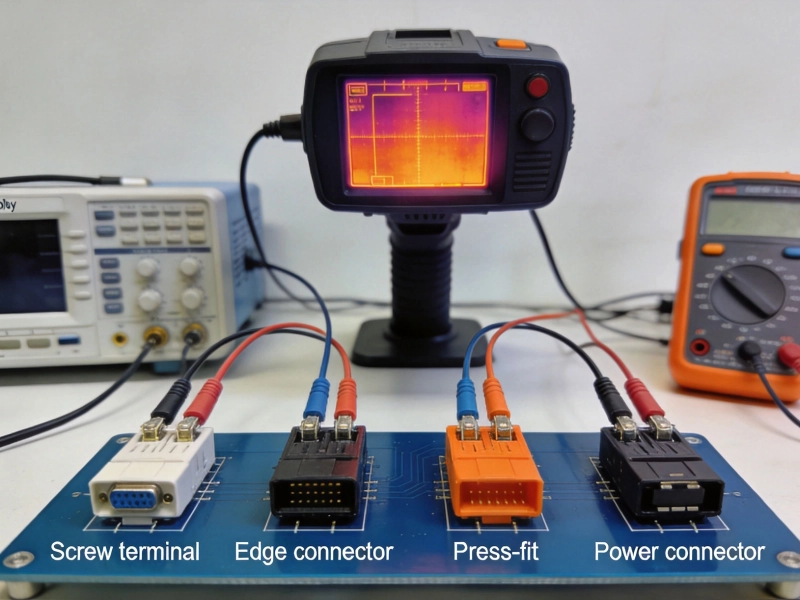
High Current PCB Connector Selection: Test Results and Real Performance DataMay/21/2026
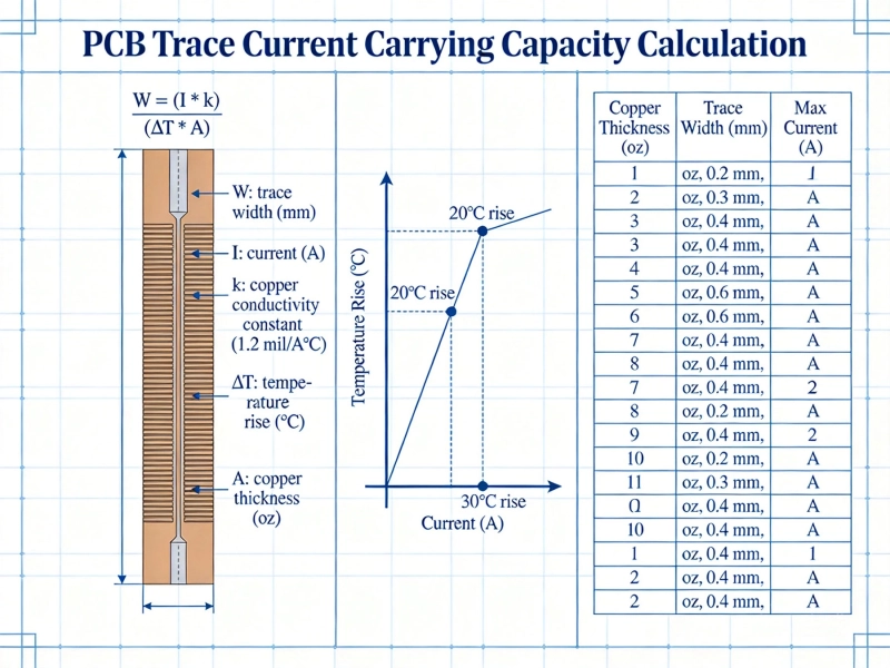
IPC-2152 Current Carrying Capacity: The Definitive PCB Trace Calculator GuideMay/21/2026
High Current PCB Flex-Rigid: Current Capacity in Bend AreasOctober/09/2026

High Current PCB Testing: Thermal Imaging vs. 4-Wire Kelvin MeasurementJuly/22/2026
High Current PCB Via Plating: 1mil vs. 2mil Thickness Reliability TestAugust/03/2026

High Current PCB Design for Drone ESCs: Minimizing Loop InductanceAugust/03/2026