

Power Electronics Design presents unique challenges that differ fundamentally from signal-level circuit design. When current requirements climb above 10 or 20 amps, the humble Copper Trace that works perfectly for data signals becomes a liability. Engineers designing High Current power delivery systems face a fundamental choice: use Heavy Copper traces to channel current through the PCB itself, or incorporate discrete bus bars that sit above or within the board to conduct current more efficiently. Each approach offers distinct advantages, and the right choice depends on the specific application requirements, volume economics, and manufacturing constraints.
Understanding the trade-offs between bus bars and Heavy Copper traces requires examining thermal performance, current capacity, mechanical integration, and total system cost. This comparison provides the technical framework for making that decision for your next High Current PCB project.
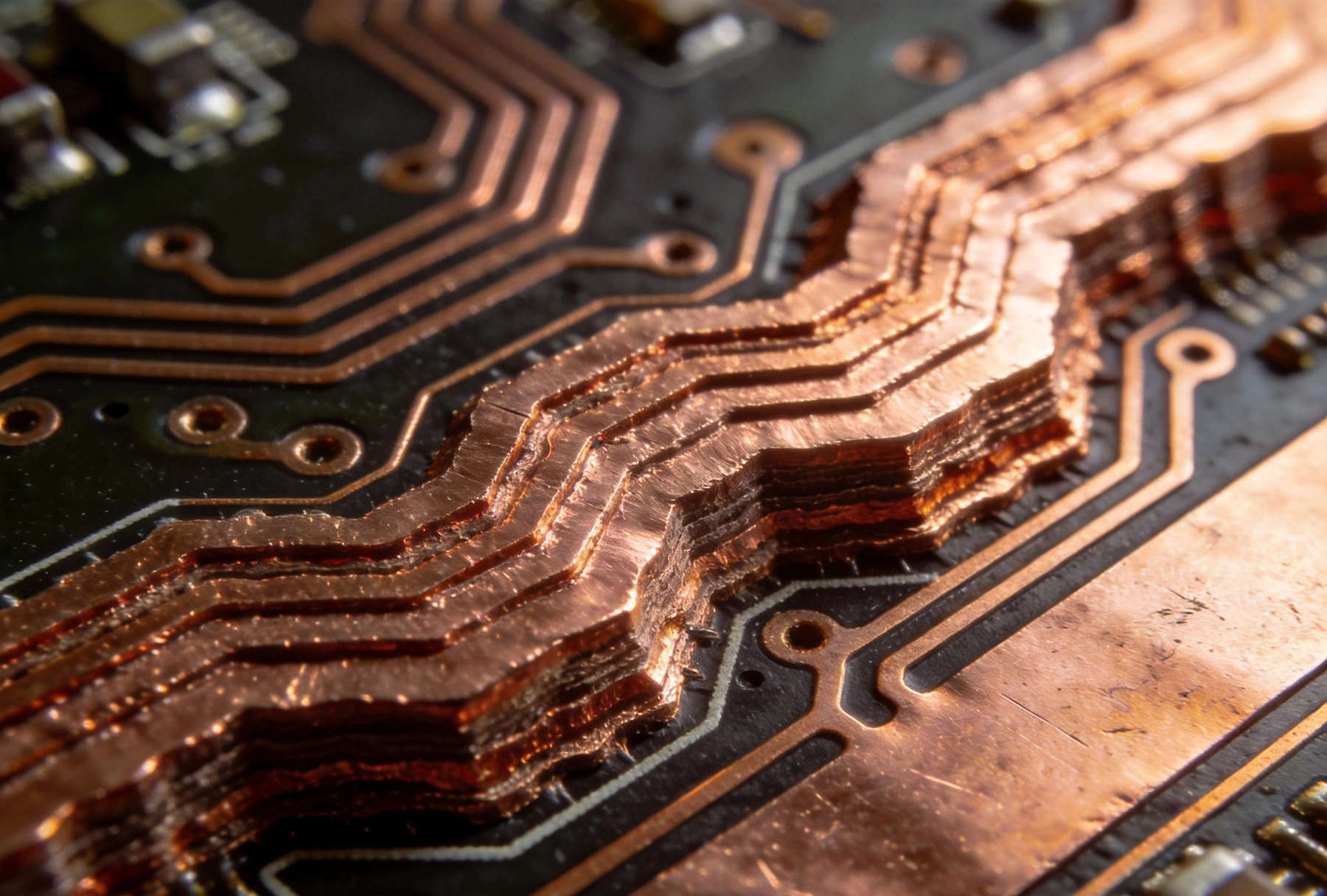
Before comparing bus bars and heavy copper traces, it is worth understanding why standard Pcb Traces become inadequate at high currents. A typical 1-ounce Copper Trace—one ounce of copper per square foot, approximately 1.4 mils thick—has a resistance that generates significant heat when carrying more than a few amps of continuous current. The heat generated follows Ohm's law: power equals current squared times resistance. As current increases, the power dissipated in the trace grows exponentially, quickly exceeding what the board can dissipate without overheating.
Temperature rise in a trace is determined by the balance between heat generated and heat dissipated to the surrounding environment. At some current level, this balance tips toward unacceptable temperature rise, causing the trace itself, nearby components, and the board substrate to exceed their maximum rated temperatures. The only ways to reduce temperature rise are to lower resistance, improve thermal dissipation, or both.
Heavy copper traces reduce resistance by increasing cross-sectional area. Doubling trace thickness halves resistance, allowing the same current to flow with half the heat generation. Similarly, widening a trace reduces resistance proportionally. For applications requiring 20 to 50 amps, traces that are 4 to 10 mils thick and hundreds of mils wide become necessary—dimensions that push the limits of standard PCB Fabrication.
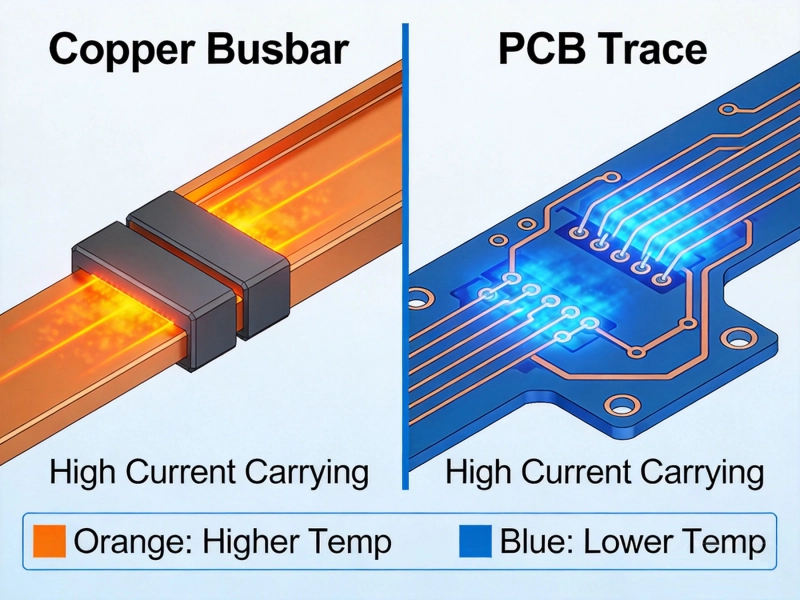
Bus bars provide an alternative path by using solid metal conductors with cross-sectional areas orders of magnitude larger than any practical Pcb Trace. A Bus Bar with a cross-section of 5mm by 1mm carries more current with less resistance and less heating than the heaviest practical copper trace on a standard board.
Heavy copper PCB Fabrication extends standard processes to achieve trace thicknesses ranging from 3 ounces per square foot up to 20 ounces or more. Standard PCB processing can accommodate copper weights up to approximately 6 ounces relatively easily, with specialized facilities capable of achieving much heavier builds through differential plating or sequential lamination.
The primary advantage of heavy copper traces is their integration within the PCB structure itself. Traces are defined photolithographically, just like standard copper features, meaning they inherit the precise geometry and registration that PCB processes provide. No additional assembly steps are required to create High Current paths—the heavy copper is part of the board from the moment it leaves the fabrication line.
Thermal Vias play a critical role in heavy copper trace design for high current applications. Placing Thermal Vias beneath large current-carrying traces transfers heat from the component side to internal ground planes or bottom-side heat spreading layers. The heat spreading effect of internal planes significantly improves thermal performance, allowing heavier currents to be carried without excessive temperature rise.
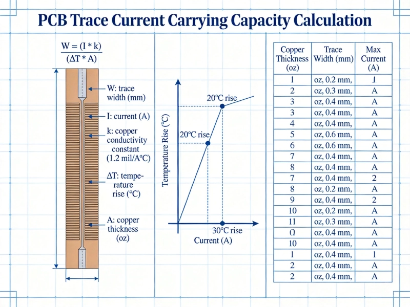
Trace width calculations for heavy copper must account for temperature rise limits specified by the application. Ipc-2152 provides baseline guidance for current-carrying capacity, but these charts assume uniform Heat Dissipation conditions that rarely match real-world applications. For boards with internal planes, restricted airflow, or elevated ambient temperatures, derating factors of 50% or more from IPC baseline values are commonly applied.
Bus bars are discrete metal conductors—typically copper or aluminum—that are mounted to or laminated within a Pcb Assembly to carry high current between components. Unlike traces, bus bars are manufactured as separate components and installed during the board assembly process, adding fabrication and assembly complexity but enabling current capacity that no Pcb Trace can match.
The most common Bus Bar configurations include surface-mounted copper strips that sit above the board, laminated bus bars where copper is bonded to the PCB surface, and embedded bus bars where the conductor is placed between PCB layers during lamination. Each configuration offers different trade-offs in current capacity, thermal performance, and manufacturing complexity.
Surface-mounted bus bars are the simplest implementation, using copper bars or strips that are soldered to PCB pads in the same process used for other components. These bus bars can be bent, shaped, and oriented to route current around obstacles on the board, providing routing flexibility that integrated traces cannot match. However, they add height above the board surface, which may conflict with enclosure or shielding requirements.
Laminated and embedded bus bars offer lower profile solutions by integrating the conductor into or onto the PCB structure. Laminated bus bars attach copper sheets to the board surface with adhesive or solder, creating a flat high-current plane. Embedded bus bars sit between PCB layers, completely hidden within the board stackup. These configurations provide the cleanest profile but require specialized fabrication processes that significantly increase cost and lead time.
Thermal Management is often the primary driver for choosing bus bars over heavy copper traces. The fundamental thermal advantage of bus bars stems from their larger cross-sectional area, which provides lower resistance and therefore lower heat generation per amp of current carried.
For a given current and ambient temperature, a properly sized bus bar will run cooler than an equivalent heavy copper trace. This thermal advantage translates into higher Current Density capability, smaller conductor size, or both. In applications where board space is constrained, bus bars may be the only viable solution for achieving required current ratings.
Heavy copper traces, however, benefit significantly from the thermal mass and connectivity of the PCB itself. A trace on a multi-layer board with solid ground and Power Planes can dissipate heat through the entire board structure, spreading thermal load across a large area. Bus bars, particularly surface-mounted types, dissipate heat primarily through their connection points to the PCB, creating localized thermal concentrations that must be managed.
The effective thermal path differs between the two approaches. Heavy copper traces spread heat into the board substrate and adjacent copper planes. Surface bus bars rely on solder joints and thermal vias to transfer heat into the board structure. The optimal choice depends on where the heat needs to go in your specific system, and whether the PCB itself is thermally managed through Heat Sinks, airflow, or thermal planes.
Current capacity is the most straightforward comparison between bus bars and heavy copper traces, but the numbers depend heavily on specific geometry, cooling conditions, and acceptable temperature rise. General guidelines can establish relative capability, but actual design must account for specific application parameters.
A 6-ounce copper trace, which represents the practical upper limit for standard PCB processing, can typically carry approximately 30 to 40 amps with a 20 to 30 degree Celsius temperature rise under natural convection conditions. Achieving higher current with traces requires specialized processing or multi-track paralleling, which adds complexity.
Bus bars, by contrast, can carry hundreds of amps with manageable temperature rise. A Copper Bus Bar with a cross-section of 10mm by 2mm routinely carries 200 to 300 amps. The Current Density achievable depends on cooling—forced air cooling or liquid cooling can dramatically increase current capacity for both approaches, but the relative advantage of bus bars grows as current requirements increase.
Voltage drop across the current-carrying path deserves careful attention in high current designs. Even small resistances accumulate significant voltage drop at high currents. A 10-milliohm resistance that is negligible at 100 milliamps drops 1 volt at 100 amps, which may be unacceptable in power delivery applications. Bus bars with their lower resistance per unit length generally provide superior voltage drop performance, particularly over longer distances.
Cost comparison between heavy copper traces and bus bars involves multiple factors that shift in relative importance depending on volume, board complexity, and current requirements.
Heavy Copper Pcb fabrication adds incremental cost over standard boards due to additional plating steps, longer processing times, and tighter process controls required for uniform Copper Thickness. The per-board cost premium for heavy copper ranges from modest premiums for 3 to 4 ounce builds to substantial premiums for 10 ounce and heavier constructions. Beyond approximately 6 ounces, standard PCB processing reaches its practical limit, and achieving heavier copper requires differential plating techniques that add significant cost and complexity.
Bus bars introduce separate component costs, additional assembly steps, and specialized fabrication processes. Laminated or embedded bus bars require additional manufacturing operations that add substantial cost. Surface bus bars are less expensive but still add component and assembly costs. However, bus bars may enable a simpler overall board design by reducing layer count or eliminating parallel trace arrangements, potentially offsetting their direct cost.
At lower current levels—say 20 to 50 amps—heavy copper traces are almost always more cost-effective. The incremental cost of heavy copper processing is lower than the combined cost of bus bar components and assembly. As current requirements increase beyond this range, bus bars become increasingly competitive on total system cost because achieving equivalent current capacity with traces requires multiple parallel paths that consume significant board area and add complexity.
Both heavy copper traces and bus bars present DFM challenges that must be addressed during the design phase to ensure producible and reliable products.
For heavy copper designs, registration accuracy between layers becomes more challenging as Copper Weight increases. Heavy copper features can shift slightly during lamination due to flow of prepreg resin, requiring wider tolerances for Annular Ring and registration specifications. Panel flatness may also be affected, which matters for assemblies that require uniform paste deposition or automated Component Placement.
Plating uniformity in heavy copper PCBs requires careful process control. The plating chemistry must be managed to achieve consistent Copper Thickness across large panel areas and inside vias. Uneven plating can create Current Distribution problems and hot spots under high current conditions. Ask your fabricator about their plating process controls and how they verify uniformity on heavy copper orders.
Bus bar designs must account for thermal expansion mismatch between the Copper Bus Bar and the PCB substrate. During Thermal Cycling, the bus bar expands and contracts at a different rate than the FR-4 or polyimide base material, creating mechanical stress on solder joints. Flexible connections, controlled fillet geometry, and appropriate solder alloy selection all contribute to reliable bus bar assemblies under Thermal Cycling conditions.
Laminated bus bar designs require precise gap control between the bus bar and adjacent PCB features. Any contact between the bus bar and unintended conductive features creates a short circuit. Design rules must include adequate Creepage And Clearance distances, and fabrication processes must achieve the precision necessary to maintain these distances throughout production.
The decision between heavy copper traces and bus bars is not binary in all cases. Many high current designs use a combination of both approaches, employing heavy copper on the PCB for moderate currents and incorporating bus bars for the highest current segments of the power path. Understanding where each approach excels helps optimize the overall design.
Use heavy copper traces when your current requirements fall within the practical range of standard heavy copper processing—typically up to 30 to 50 amps per trace depending on thermal conditions. Heavy copper is also appropriate when board space is abundant and the current must be distributed across multiple connection points on the same board layer. The integration benefit of traces embedded in the board structure provides consistent thermal spreading through the PCB itself.
Consider bus bars when current requirements exceed what traces can practically handle, when routing flexibility is needed, or when minimizing voltage drop is a priority. Bus bars are particularly advantageous for carrying current between widely separated points, connecting boards to external power sources, or distributing current to multiple parallel loads. The Manufacturing Cost premium is justified when the electrical or thermal performance of bus bars solves problems that traces cannot.
Consult with your PCB fabricator and assembly partner early in the design process. Their experience with specific current, thermal, and geometric requirements will inform decisions that are difficult to make from first principles alone. Many fabricators have developed proprietary processes for heavy copper that push the practical limits of standard approaches, potentially eliminating the need for bus bars in applications where they might otherwise seem necessary.
Choosing between High Current Pcb bus bars and heavy copper traces is a systems-level decision that affects Thermal Management, mechanical packaging, Manufacturing Cost, and reliability. Neither approach is universally superior; the right choice depends on specific current requirements, board constraints, thermal environment, and volume economics. By understanding the fundamental trade-offs outlined here, engineering teams can make informed decisions that optimize performance and cost for their particular application.
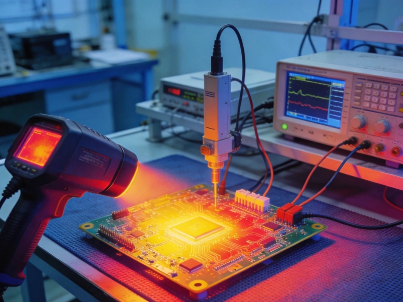
High Current PCB Testing: Thermal Imaging vs. 4-Wire Kelvin MeasurementJuly/22/2026
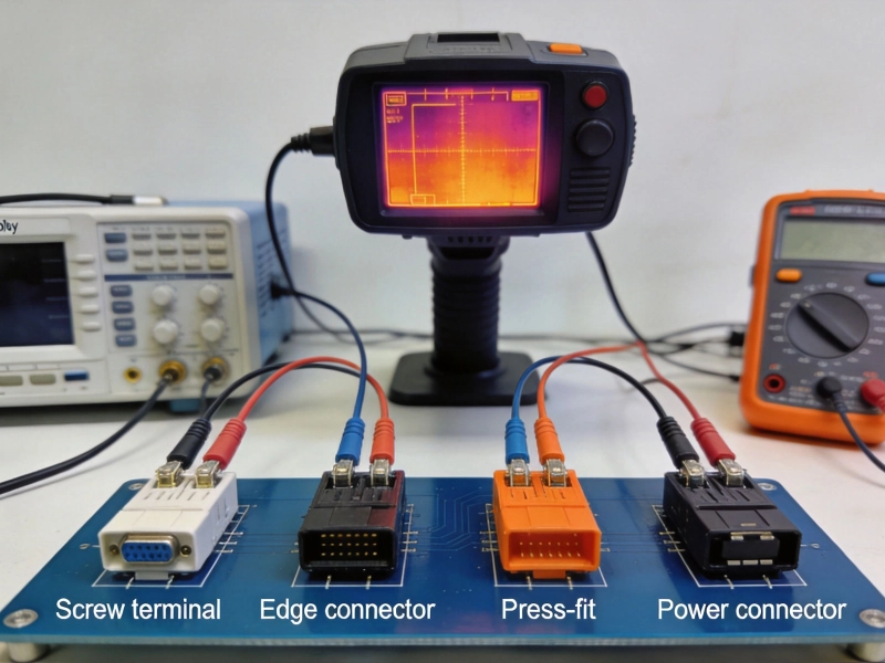
High Current PCB Connector Selection: Test Results and Real Performance DataMay/21/2026
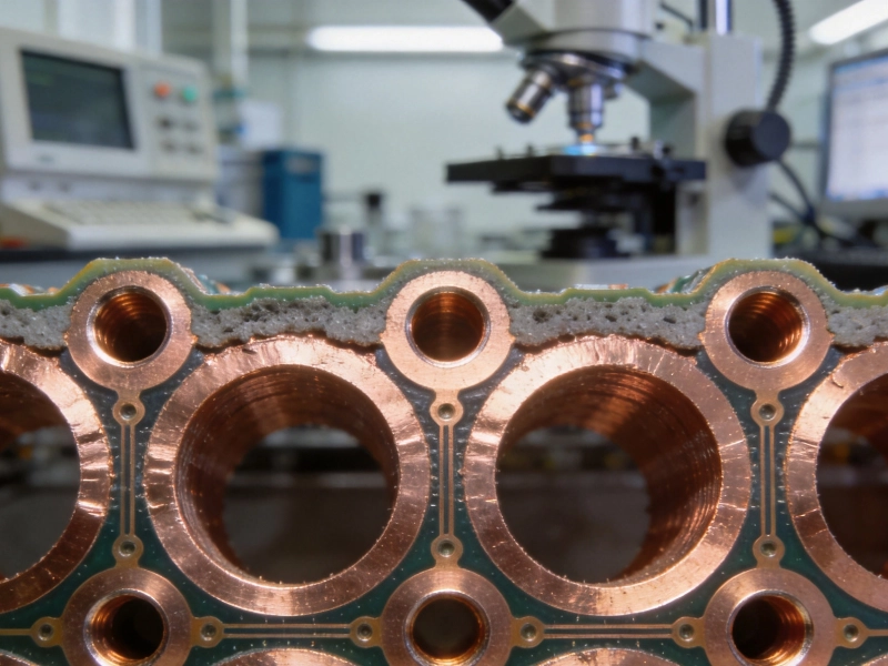
High Current PCB Via Plating: 1mil vs. 2mil Thickness Reliability TestAugust/03/2026
Bus Bar vs PCB Trace for High CurrentMay/21/2026
High Current PCB Decoupling Caps: Placement Distance vs. Loop AreaOctober/12/2026
High Current PCB Flex-Rigid: Current Capacity in Bend AreasOctober/09/2026
High Current PCB Annular Rings: Minimum Size vs. Reinforced SizeAugust/12/2026
IPC-2152 Current Carrying Capacity: The Definitive PCB Trace Calculator GuideMay/21/2026