

High Current printed circuit board design presents unique challenges that go far beyond simple width calculations based on current requirements. One of the most critical yet often overlooked aspects involves current crowding effects at trace transitions, particularly where conductors make sharp turns or abrupt changes in direction. The choice between sharp corners and teardrop transitions significantly impacts Current Distribution, thermal performance, and overall reliability of high-power circuits. Understanding the physics of current crowding and implementing proper design techniques becomes essential for engineers designing power supplies, motor controllers, battery management systems, and other high-current applications where reliability and Thermal Management are paramount. This analysis explores the fundamental differences between sharp corner and teardrop approaches, providing practical guidance for optimizing High Current PCB designs.
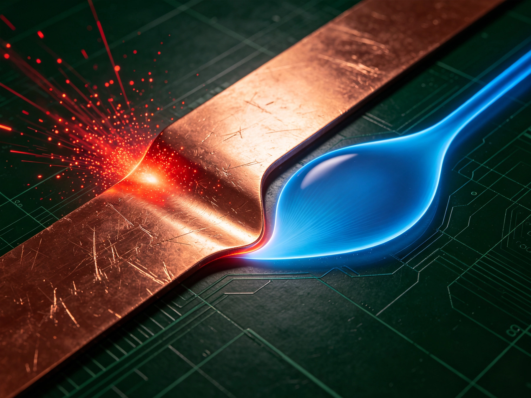
Current crowding represents a fundamental electrical phenomenon where Current Density becomes non-uniform across a conductor's cross-section. In High Current applications, this effect becomes particularly pronounced at geometric discontinuities including bends, corners, and transitions. When current flows through a straight conductor, Current Distribution remains relatively uniform across the cross-section due to the skin effect and proximity effects at higher frequencies. However, when the conductor makes a sharp turn, the outer edge of the bend becomes significantly longer than the inner edge, creating a resistance differential that forces more current toward the shorter, lower-resistance inner path. This concentration of current at the inner corner dramatically increases Current Density at that point, creating localized heating and potential reliability issues. The current crowding factor—the ratio of maximum current density to average current density—can exceed 3:1 at sharp 90-degree corners in high current applications, meaning the inner corner carries three times the average current density of the trace. Understanding this phenomenon represents the first step toward implementing effective mitigation strategies in High Current PCB design.
Sharp corner design represents the traditional approach to PCB routing, characterized by 90-degree or acute angle turns without any geometric modification at the transition point. This approach offers simplicity in layout implementation, minimal board space consumption, and straightforward CAD design processes. However, sharp corners create several significant disadvantages in high current applications. The inner corner radius approaches zero, creating extreme current crowding with current densities reaching dangerous levels. Thermal effects concentrate at the inner corner, creating hot spots that can exceed safe operating temperatures for copper traces and solder joints. The effective current-carrying capacity reduces dramatically at corners, meaning trace width calculations based on straight conductor characteristics become invalid. Mechanical stress concentrates at sharp corners, making traces more susceptible to cracking under Thermal Cycling and mechanical vibration. Manufacturing challenges increase as etching processes struggle to maintain consistent trace widths at acute angles, potentially creating weak points. These limitations become progressively more severe as current levels increase and applications demand higher reliability, making sharp corners increasingly problematic for modern High Current Pcb Design.
Teardrop transitions represent a geometric solution designed specifically to mitigate current crowding effects at trace transitions. The teardrop shape gradually widens the trace as it approaches a pad, via, or transition point, creating a smooth, continuous transition that maintains more uniform current distribution. The design typically features a curved outer boundary that expands from the trace width to a maximum width at the transition point, then contracts symmetrically to the destination conductor width. This geometric modification provides several critical benefits in high current applications. Current density distribution becomes significantly more uniform across the transition region, reducing peak current densities by 30-50% compared to sharp corners. Thermal characteristics improve as heat distributes more evenly across a larger surface area, reducing peak temperatures and thermal gradients. Effective current-carrying capacity increases at transition points, allowing traces to maintain their rated current capacity throughout the entire length. Mechanical strength enhances as the gradual transition distributes stress more effectively, reducing susceptibility to cracking and fatigue failure. Manufacturing reliability improves as etching processes produce more consistent results with gradual geometric changes. These benefits make teardrop transitions an essential tool for engineers designing high current PCBs with demanding reliability requirements.
Thermal performance represents one of the most significant differences between sharp corner and teardrop transition designs in high current applications. Sharp corners create localized hot spots where temperatures can exceed the average trace temperature by 20-40°C or more, depending on current level and thermal conditions. These hot spots accelerate thermal degradation of copper traces, solder joints, and adjacent components, potentially reducing product lifespan dramatically. Finite element analysis (FEA) simulations comparing thermal profiles show sharp corners creating temperature gradients exceeding 15°C across just a few millimeters of trace length, while teardrop transitions maintain gradients below 5°C across the same distance. The reduced thermal gradient in teardrop designs provides multiple benefits: slower thermal aging of materials, reduced thermal stress on solder joints, more predictable thermal performance, and improved reliability in high-temperature environments. Experimental testing under controlled conditions demonstrates that teardrop transitions can reduce peak operating temperatures by 15-25% compared to equivalent sharp corner designs at the same current level. This temperature reduction directly translates to improved reliability, as many failure mechanisms follow Arrhenius kinetics where failure rates approximately double for every 10°C temperature increase. For high current applications operating near thermal limits, this temperature difference can make the difference between acceptable reliability and premature failure.
Current capacity calculations for high current traces must account for transition effects when comparing sharp corners versus teardrop designs. Standard Ipc-2152 calculations assume uniform current distribution along straight conductors and don't adequately address current crowding at transitions. For sharp corners, engineers must apply derating factors typically ranging from 20-40% depending on current level, trace width, and ambient conditions. A trace that theoretically carries 10A based on Ipc-2152 may only safely carry 6-8A when making sharp 90-degree corners. Teardrop transitions, in contrast, can maintain 90-95% of the theoretical current capacity at transition points when properly designed. The current carrying benefit becomes particularly significant in high current applications where board space is limited and every millimeter of trace width matters. Design calculations for high current PCBs should incorporate transition-specific factors including: Trace Geometry modification at transitions (accounting for teardrop expansion), multiple transition analysis (when traces make multiple turns), Copper Weight variations (inner versus outer layers), thermal conductivity of adjacent materials, and ambient environmental conditions. Sophisticated simulation tools including 2D and 3D electromagnetic field analysis help predict current distribution and identify potential hot spots before committing to fabrication. These analytical approaches become essential for optimizing high current designs while minimizing board area and manufacturing costs.
Mechanical reliability represents another critical area where sharp corners and teardrop transitions diverge significantly. High current PCBs often operate in environments subject to Thermal Cycling, vibration, and mechanical stress that challenge the mechanical integrity of copper traces and solder joints. Sharp corners create stress concentration points where mechanical stress localizes during thermal expansion and contraction. The stress concentration factor at a sharp 90-degree corner can exceed 3:1, meaning the inner corner experiences three times the average mechanical stress across the trace. Over repeated thermal cycles, this stress concentration can initiate and propagate cracks, leading to eventual trace failure even when electrical performance appears acceptable. Teardrop transitions distribute mechanical stress more evenly across a larger area, reducing peak stress concentrations by 40-60% compared to sharp corners. This stress reduction translates directly to improved mechanical reliability: longer operational lifespan under thermal cycling, reduced susceptibility to vibration-induced failures, better resistance to mechanical shock, and improved performance in automotive and industrial applications where environmental stress is severe. Mechanical reliability testing conducted under accelerated life conditions demonstrates that teardrop transitions can extend mean time to failure (MTTF) by 2-3 times compared to equivalent sharp corner designs in high current applications. This reliability improvement becomes particularly important for applications where maintenance access is difficult or where downtime costs are prohibitive.
Implementing teardrop transitions in High Current Pcb designs requires careful attention to manufacturing constraints and design tool capabilities. While teardrop shapes provide superior electrical and thermal performance, they consume additional board space that must be accommodated in layout planning. Typical teardrop expansions add 20-40% to trace width at transition points, requiring designers to account for this increased space in board layout. Most modern Pcb Design CAD tools include automated teardrop generation features that can apply appropriate teardrop shapes to pads, vias, and transitions based on design rules. When implementing teardrops manually, designers should maintain smooth curves with minimum radii that accommodate manufacturing capabilities—typically 0.2-0.3mm minimum inner radius for standard PCB processes. Manufacturing considerations include: etching process capabilities (ensuring teardrop shapes are faithfully reproduced during etching), drill registration accuracy (for vias where teardrops connect), copper plating consistency (ensuring uniform Copper Thickness across teardrop regions), and inspection requirements (verifying that teardrop shapes meet design specifications). High current applications often require enhanced copper plating (3oz or higher) and specialized plating processes to ensure adequate current capacity in teardrop regions. Collaboration with PCB fabricators early in the design process helps ensure that teardrop designs are manufacturable and that fabrication processes can consistently achieve the required geometries and tolerances. Proper implementation of teardrop transitions represents a balance between electrical performance, manufacturing capability, and cost considerations.
Different high current applications present varying requirements that influence the choice between sharp corners and teardrop transitions. For automotive Power Electronics applications requiring extended operational life and exposure to temperature extremes, teardrop transitions should be used at all critical high-current transitions, particularly for power stage output traces, motor phase outputs, and battery charge/discharge paths. In industrial Motor Controller applications subject to vibration and thermal cycling, teardrops provide essential reliability benefits at motor driver outputs, brake resistor connections, and DC bus interconnects. For server power supply and telecommunications Power Distribution applications where reliability is paramount but board space is constrained, teardrops should be prioritized for primary power paths and highest current traces, while sharp corners may be acceptable for lower current control signals. In consumer electronics battery management systems where size constraints are extreme, selective use of teardrops at the highest current transition points provides optimal balance between space utilization and reliability. Medical device power systems operating at near-ambient temperatures with moderate current levels may use teardrops at all power-related transitions to ensure maximum reliability and safety. These application-specific guidelines should be adapted based on specific current levels, environmental conditions, reliability requirements, and cost constraints. The key principle is to prioritize teardrop transitions where current crowding effects are most severe and where reliability requirements are highest.
Beyond basic teardrop transitions, advanced High Current Pcb Design incorporates additional techniques to further mitigate current crowding effects and improve overall performance. Multi-corner smoothing techniques replace sharp 90-degree turns with sequences of smaller angle turns (45-degree or 30-degree) that gradually change direction, reducing current crowding at individual corners. Meandered trace designs distribute current across multiple parallel paths, reducing current density in any single conductor while maintaining flexibility in layout routing. Thick copper layers (3oz, 4oz, or higher) provide increased cross-sectional area that helps reduce current density and thermal gradients, though they require specialized fabrication processes. Copper pours connected to traces act as Heat Sinks that distribute thermal energy more effectively and provide alternative current paths that reduce crowding. Through-hole via arrays connect multiple layers in parallel, effectively increasing current capacity at transition points while distributing current across a larger cross-section. Surface mount Component Placement strategies position high-current components to minimize trace length and reduce the number of transitions, decreasing opportunities for current crowding effects. Thermal Analysis tools including infrared thermography and computational fluid dynamics (CFD) simulation identify hot spots and guide optimization of transition geometries. These advanced techniques, combined with fundamental teardrop transition principles, enable designers to create high current PCBs that meet demanding performance and reliability requirements while optimizing board space and manufacturing costs.
The choice between sharp corners and teardrop transitions in High Current Pcb design represents far more than an aesthetic preference—it's a fundamental decision affecting current distribution, thermal performance, mechanical reliability, and overall product success. While sharp corners offer simplicity and space efficiency, they create current crowding effects that can lead to localized heating, accelerated degradation, and premature failure in high current applications. Teardrop transitions provide an effective geometric solution that significantly reduces current crowding, improves thermal characteristics, enhances mechanical strength, and increases reliability. For engineers designing high current PCBs, understanding the physics of current crowding and implementing appropriate mitigation techniques becomes essential for creating products that meet demanding performance and reliability requirements. The additional board space and design complexity required for teardrop transitions represent a worthwhile investment that pays dividends in improved reliability, reduced warranty costs, and enhanced customer satisfaction. As electronic systems continue to push current carrying capabilities higher and reliability requirements more demanding, proper attention to current crowding effects through geometric design will remain a critical factor in successful high current Pcb Design.
What is current crowding in high current PCBs?
Current crowding occurs when current density becomes non-uniform across a conductor's cross-section, typically at geometric discontinuities like sharp corners. At sharp turns, the inner edge of the bend is shorter than the outer edge, creating lower resistance that forces more current to concentrate at the inner corner. This can increase current density at that point by 3x or more compared to the average trace density, creating localized heating and reliability issues.
How do teardrop transitions improve thermal performance?
Teardrop transitions gradually widen traces at transition points, creating smooth geometric changes that maintain more uniform current distribution. This reduces peak current densities by 30-50% compared to sharp corners, leading to more even heat distribution across a larger surface area. Testing shows teardrops can reduce peak operating temperatures by 15-25% compared to equivalent sharp corner designs at the same current level.
When should I use teardrop transitions versus sharp corners?
Teardrops should be used for all high current transitions (typically 5A and above), particularly in automotive, industrial, medical, and other applications requiring high reliability. Sharp corners may be acceptable for low current signal traces (<2A) in consumer applications where space constraints are extreme and reliability requirements are moderate. The highest priority for teardrops is at points where current density is highest and reliability impact is greatest.
How much additional board space do teardrop transitions require?
Teardrop expansions typically add 20-40% to trace width at transition points. The exact space requirement depends on trace width, current level, and teardrop geometry. Designers must account for this increased space in board layout planning, particularly in dense high current designs where board space is at a premium. Most CAD tools include automated teardrop generation that calculates optimal dimensions based on design rules.
What advanced techniques complement teardrop transitions for high current designs?
Advanced techniques include multi-corner smoothing using smaller angle turns, meandered trace designs for current distribution, thick copper layers (3oz+), copper pours as Heat Sinks, through-hole via arrays for parallel paths, strategic Component Placement to minimize transitions, and Thermal Analysis tools for optimization. These techniques work synergistically with teardrops to create robust high current PCB designs that meet demanding performance requirements.
High Current PCB Grounding: Star Ground vs. Ground Plane in High Current PathsJuly/31/2026
High Current PCB Solder Wicking: Tented Vias vs. Untented ViasSeptember/01/2026

High Current PCB Ceramic Substrates: DBC vs. AMB Performance ComparisonOctober/14/2026
High Current PCB Surface Finish: ENIG vs. HASL for High Current PadsSeptember/23/2026
Overcoming Voltage Drop in High Current PCB Power Planes: A Case StudyJuly/13/2026
High Current PCB Routing: 45-Degree Angles vs. Curved Traces in PracticeJuly/12/2026
High Current PCB Annular Rings: Minimum Size vs. Reinforced SizeAugust/12/2026
Plated Through Hole Current Rating for PCBsJune/10/2026