

Solar inverters operate at the heart of photovoltaic systems, converting DC power from panels into AC power for homes and grids. This conversion process demands PCB designs that can handle substantial current flows — sometimes exceeding 50 or even 100 amps — without overheating, voltage drop, or premature failure. Designing PCBs for these conditions requires a fundamentally different approach than typical signal-layer boards.
If you're designing a solar inverter and treating the PCB like a standard microcontroller board, you're setting yourself up for problems. High Current introduces thermal challenges, electromigration risks, and electromagnetic effects that don't appear in low-power designs. This guide walks through everything you need to know to create reliable, efficient inverter PCBs that perform year after year in demanding solar installations.
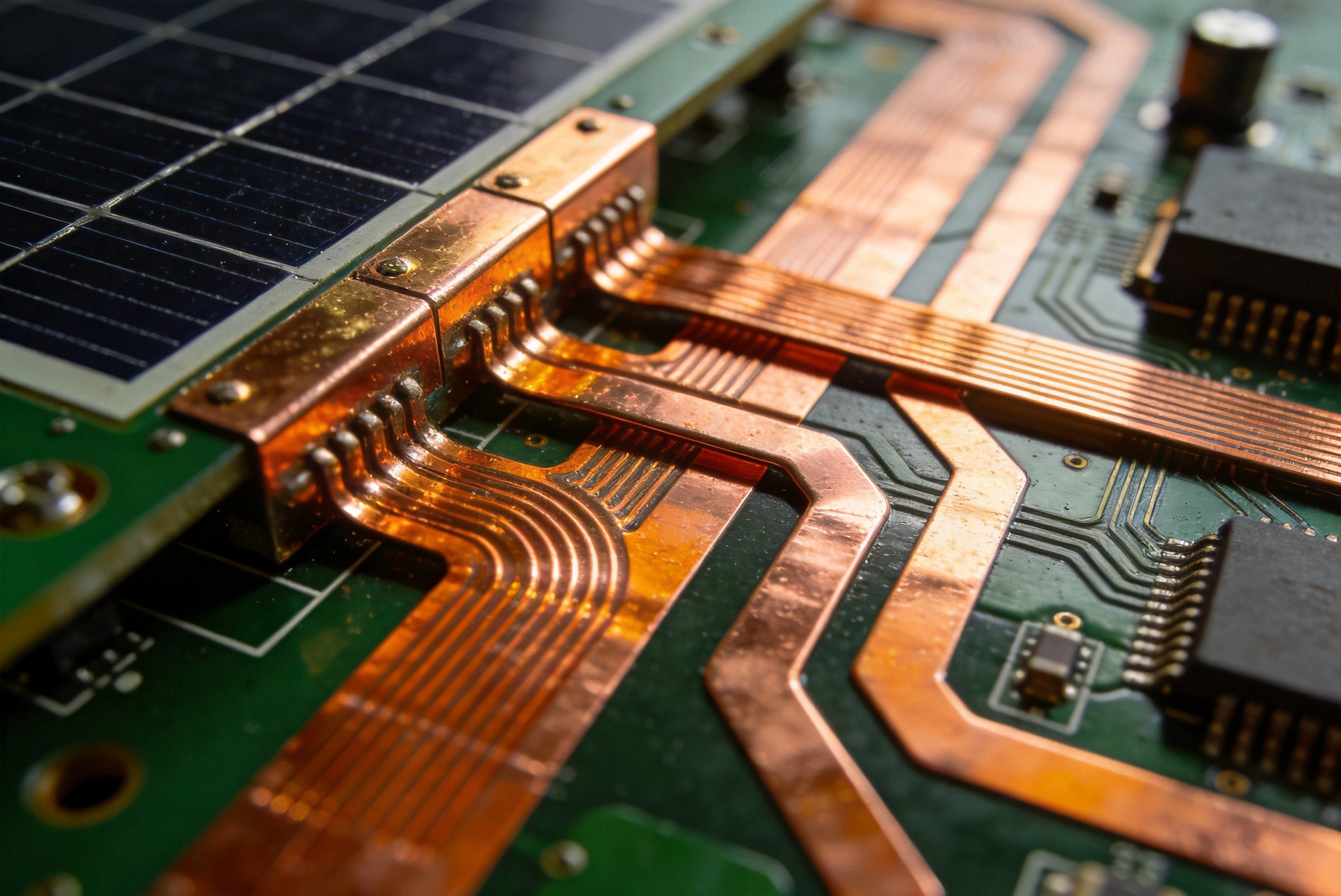
When current travels through a conductor, it generates heat proportional to the square of the current and the resistance of the path. This relationship — P = I²R — becomes the governing equation for every design decision in high-current sections of a solar inverter. At 50 amps flowing through a poorly sized trace, you're dissipating enough heat to destroy components if the thermal path isn't properly managed.
Beyond simple heating, high currents create voltage drop across resistive paths. In a solar inverter, this matters directly for efficiency — every milliohm of extra resistance in the power path represents lost energy that never reaches the grid. At peak output currents, even 10 milliohms of excess resistance can waste several watts in a residential inverter, degrading efficiency and generating unnecessary heat.
Electromigration represents another silent failure mechanism. When electrons collide with copper atoms in a conductor, they gradually push atoms in the direction of current flow. At High Current densities — typically above 10² A/cm² — this effect accelerates, eventually creating voids in the conductor that increase resistance and generate more heat in a destructive spiral. High-current Pcb Traces must be designed to keep Current Density well below electromigration thresholds.
Determining appropriate trace width for high-current paths isn't guesswork. The Ipc-2152 standard provides the foundational reference for current-carrying capacity in PCBs, establishing relationships between conductor width, thickness, temperature rise, and current capacity. For solar inverter applications, you typically want to limit temperature rise to 10-20°C above ambient under worst-case operating conditions.
Basic calculations start with understanding your Copper Weight. Standard PCB copper comes in weights from ½ oz per square foot (18 microns thick) to 3 oz or more. For high-current inverter traces, you'll almost always want at least 2 oz copper, and many designs use 3 oz or heavier for main power paths. The relationship isn't linear — doubling Copper Thickness more than doubles current capacity because it also improves Heat Dissipation through the copper itself.
For a practical example, consider a 50-amp trace on a typical solar inverter main bus. At 2 oz copper, you might need a 250-mil (6.35mm) trace to stay within a 20°C temperature rise budget. That's a wide trace by most PCB standards, and it will consume significant board area. Some designers route these as dedicated bus bars on separate layers or use external bus bars entirely.
Online calculators provide reasonable starting points, but always validate against your specific thermal environment. A trace that works fine in a well-ventilated enclosure might fail in a sealed, sun-heated solar inverter cabinet. Consider worst-case ambient temperatures — a rooftop inverter in Arizona faces very different thermal conditions than one in Germany.
Thermal Management separates successful High-current Pcb designs from ones that fail prematurely. The goal isn't just removing heat — it's distributing it evenly so that no single component or trace becomes a hotspot that limits overall system performance.
Thermal Vias provide one of the most effective tools for heat management in inverter PCBs. Placing Thermal Vias under MOSFETs, IGBTs, and other power semiconductors creates a low-resistance thermal path from the component to internal ground planes or external Heat Sinks. For a TO-247 or similar through-hole package, a cluster of 3x3 or 4x4 thermal vias under the drain tab dramatically reduces junction temperature.
These thermal vias work best when filled with thermally conductive epoxy or plated flush. Unfilled vias can actually trap air and reduce thermal performance, so specify filled and capped vias for thermal applications. Via-in-pad construction, where the via connects directly to the component pad, provides the shortest thermal path but requires careful process control during manufacturing.
Copper Pour and plane layers serve dual purposes in high-current designs. They provide low-resistance current paths while simultaneously acting as heat spreaders that distribute thermal energy across larger areas. A solid ground plane under high-current traces can reduce effective trace resistance while keeping temperatures manageable. Connect planes to power components through multiple vias to minimize Thermal Resistance at the interface.
For designs approaching 100 amps or higher, consider metal-core PCBs (MCPCBs) or IMS (insulated metal substrate) constructions. These substrates have aluminum or copper cores with high thermal conductivity, allowing heat to spread directly through the board material rather than relying solely on surface traces and vias. IMS boards commonly achieve thermal conductivity 5-10x higher than standard FR4.
Beyond a certain current level — typically 30-50 amps depending on your efficiency targets — routing power through standard Pcb Traces becomes impractical. Bus bars fill this gap, providing low-resistance paths that can handle hundreds of amps while offering predictable, manageable thermal behavior.
PCB-mounted bus bars come in several forms. Discrete bus bars are separate metal components — often tin-plated copper — that get soldered or bolted to the PCB. These provide the lowest resistance and highest current capacity but add assembly complexity and component cost. Popular options include laminated bus bars with insulation layers between conductor strips, providing controlled impedance along with high current capacity.
Integrated PCB bus bars use extra-thick copper plating or added copper to create on-board conductors. This approach maintains the advantages of Pcb Manufacturing — consistent quality, automated assembly — while achieving higher current capacity than standard traces. 6 oz, 10 oz, or even heavier copper constructions enable current paths that would be impossible with standard 1-2 oz boards.
When designing Bus Bar connections, pay attention to termination points. Every connection point introduces resistance and potential hot spots. Solder joints must be sized for the current they carry, with sufficient pad size and solder volume to create reliable, low-resistance connections. Bolted connections need proper torque specifications and consideration of galvanic compatibility between materials.
Bus Bar routing should minimize sharp corners. Current Density increases at corners, and this effect becomes significant at high currents. Use radius turns rather than 90-degree angles where possible. When space constraints require sharp turns, add extra copper width around the corner or use multiple angled segments rather than a single right-angle bend.
High-current Pcb Design demands careful attention to ground plane integrity. In an inverter, the DC input ground, AC output ground, and signal ground often need careful separation to prevent noise coupling while still maintaining safety ground connections. Getting this wrong creates Emi problems, measurement errors, and potential safety hazards.
The concept of a clean signal ground versus a noisy power ground takes on literal meaning in inverter designs. Sensitive measurement circuits — current sense amplifiers, voltage sensing for MPPT tracking — need quiet reference points that don't shift with high-current switching transients. These grounds should connect to the main power ground at a single point, often called a star ground, to prevent high-frequency noise from power devices corrupting measurement signals.
Kelvin connections become essential for current sensing. When you're measuring 50 amps to implement overcurrent protection or optimize efficiency, the voltage drop across your sense resistor shouldn't be affected by currents flowing in adjacent traces. Four-wire (Kelvin) sense connections keep the measurement circuit isolated from high-current paths, providing accurate readings regardless of how other traces are routed.
Switching node layout deserves special attention because of its dual high-current and high-frequency characteristics. The inverter's MOSFETs or IGBTs switch at frequencies ranging from 10 kHz to 100 kHz or higher, creating dv/dt and di/dt transients that couple into nearby circuits. Keep switching nodes compact, route them away from sensitive signals, and use gate drive circuits that minimize Loop Area for the switching transients.
Component choices in high-current sections of an inverter PCB significantly impact both performance and reliability. While your signal components might be standard 0402 or 0603 passives, power sections demand components rated well beyond the nominal operating current.
MOSFETs and IGBTs carry the main switching current and need careful selection. Look beyond just the on-resistance specification — consider the Thermal Resistance from junction to case, the SOA (Safe Operating Area) for your switching pattern, and the body's ability to handle pulsed currents. Silicon carbide (SiC) MOSFETs increasingly dominate solar inverter designs because of their lower switching losses and higher temperature capability compared to traditional silicon devices, despite higher per-unit costs.
Input and output capacitors see high RMS ripple currents that generate heat even when average current is low. Capacitors must be rated for the ripple current they'll experience, not just the voltage rating. Electrolytic capacitors for DC bus storage should specify ripple current ratings at the switching frequency and operating temperature of your design. Ceramic capacitors for high-frequency decoupling need careful attention to capacitance derating with voltage and temperature.
Connectors and terminals are often afterthoughts but can limit system capability. A connector rated for 30 amps that's carrying 40 amps will overheat, potentially melting the housing or creating fire hazards. Specify connectors with adequate current ratings, consider derating them to 50-75% of rated capacity for reliability, and verify that wire or PCB pad connections to the connector can actually handle the current without excessive heating.
Solar inverters must meet strict Emi standards for grid compatibility and electromagnetic compatibility. High current switching creates both conducted and radiated emissions that require careful Pcb Design to keep within regulatory limits.
Switching Loop Area directly controls radiated emissions from the inverter's power stage. Every current loop acts as a small antenna, and the field strength is proportional to loop area and current magnitude. Minimize the loop formed by the MOSFET, input capacitor, and transformer or inductor connection. This often means physically co-locating these components as tightly as possible, even at the expense of routing convenience.
Snubber circuits and EMI filters address conducted emissions that travel along power cables. Without proper filtering, the inverter's switching transients can exceed grid compatibility standards and interfere with other equipment on the same electrical circuit. Include adequate X and Y capacitors, common-mode chokes, and differential mode inductors sized for the current and frequency range of your switching signals.
Shielding can help with radiated emissions but addresses symptoms rather than causes. A well-designed PCB with proper loop area control will radiate less and be easier to filter than a poorly designed board that relies on shielding to meet emissions limits. Use shielding as a supplementary measure, not a substitute for good layout practice.
Solar inverters face demanding environmental conditions that compound the challenges of high-current operation. Outdoor installations see wide temperature swings, humidity, salt air in coastal regions, and UV exposure. These factors affect PCB materials, solder joints, and component reliability in ways that indoor electronics never encounter.
Thermal Cycling causes differential expansion between components and PCB materials, gradually fatiguing solder joints over years of operation. Solar inverters experience daily temperature cycles as well as seasonal variation — a board that sees 20°C swings daily will cycle through thousands of thermal excursions annually. Designs should use components with appropriate Thermal Cycling ratings and consider conformal coating to protect circuitry from moisture while allowing some stress relief.
Moisture sensitivity affects packages differently, but most modern components are rated MSL (Moisture Sensitivity Level) 3 or better for reflow compatibility. Beyond manufacturing, moisture can cause failures in fielded equipment if water penetrates enclosures. Specify appropriate IP (Ingress Protection) ratings for enclosures, use breathable vents with hydrophobic membranes, and consider conformal coating for boards that might see humidity exposure despite enclosure protection.
Partial discharge becomes relevant at higher voltages. Solar inverter DC bus voltages can reach 600V or more in string inverters, and at these voltages, small voids or delaminations in the PCB dielectric can experience ionization that gradually degrades insulation. Use PCB materials with appropriate CTI (Comparative Tracking Index) ratings for your voltage, specify adequate spacing between high-voltage conductors, and consider conformal coating for additional protection.
High-current inverter PCBs demand thorough testing beyond standard bring-up procedures. The interaction between thermal, electrical, and mechanical stresses creates failure modes that single-parameter testing won't catch.
Thermal imaging during operation reveals hot spots before they cause field failures. Load the inverter to rated current — or as close as manufacturing test capabilities allow — and image the board with a thermal camera. Compare results against thermal simulation predictions and look for unexpected hot spots that might indicate high-resistance joints, suboptimal thermal paths, or airflow blockages.
Current density mapping using thermal methods shows where your design is most stressed. Apply high current and let the board reach thermal equilibrium, then use thermal imaging to identify areas running hottest. These hot spots often correlate with areas of highest current density or weakest thermal path. This information guides design iterations for subsequent board revisions.
Long-term reliability testing at elevated temperature accelerates failure mechanisms. Operating the inverter at elevated ambient temperature while delivering rated current compresses years of field operation into weeks or months of accelerated testing. Monitor for gradual changes in efficiency, leakage current, or insulation resistance that might indicate incipient failures before they become catastrophic.
Designing PCBs for high-current solar inverter applications requires treating Thermal Management as a first-order design constraint, not an afterthought. Every design decision — from trace width to Component Placement to bus bar sizing — should be evaluated through both electrical and thermal lenses.
Use generous copper weights and trace widths with appropriate margins above minimum calculations. Distribute heat effectively using thermal vias, copper planes, and metal-core substrates where necessary. Keep high-current paths short and compact to minimize both resistance and radiated emissions.
Pay attention to the details that differentiate Power Electronics from signal electronics: Kelvin sense connections, star grounding, proper snubbing, and connector ratings. These details determine whether your design performs reliably over the 10-15 year lifetime expected from solar installations.
Test thoroughly under realistic conditions, using thermal imaging and long-term accelerated aging to identify weaknesses before they cause field failures. A solar inverter that fails after two years in the field damages both your reputation and the economics of the installation it serves.
For 50 amp current paths in a solar inverter, 2-3 oz copper is typically the starting point. Actual requirements depend on trace width, temperature rise budget, and thermal environment. A 50-amp trace might need 200-300 mils width at 2 oz copper to stay within a 20°C rise budget. Always calculate specifically for your design conditions rather than relying on general recommendations.
Thermal runaway occurs when heating increases current density, which causes more heating. Prevent it by designing with adequate thermal margins, using components with positive temperature coefficients where appropriate, and ensuring heat can flow away from hot spots. Temperature monitoring with automatic current reduction provides a safety net if normal thermal paths are compromised.
Metal-core PCBs offer superior thermal conductivity but at higher cost and with some manufacturing constraints. For residential inverters under 10kW with adequate convective cooling, standard FR4 with careful thermal via design often suffices. For higher power densities or confined spaces, IMS substrates provide meaningful thermal performance improvements that justify their cost premium.
Efficiency losses typically trace to excessive resistance in current paths. Common culprits include inadequate trace widths, high-resistance solder joints, loose connector terminations, and corroded or oxidized contact surfaces. Current mapping with thermal imaging identifies hot spots that indicate power dissipation. Check each connection point methodically — a single marginal joint can waste several watts at 50 amps.
Minimize switching loop area, use proper snubbing on MOSFETs and IGBTs, implement adequate EMI filtering on input and output, and separate noisy power circuits from sensitive measurement circuits. Gate drive design matters significantly — fast, clean gate transitions reduce both switching losses and EMI. Consider spread-spectrum switching techniques that distribute emissions across a frequency range rather than concentrating them at discrete harmonics.
The complexity of High-current Pcb design for solar inverters rewards methodical approaches. Start with accurate calculations, design for realistic thermal environments, choose components with appropriate ratings, and validate thoroughly before committing to production. Each of these steps adds incremental assurance that your inverter will perform reliably over its expected operational lifetime.
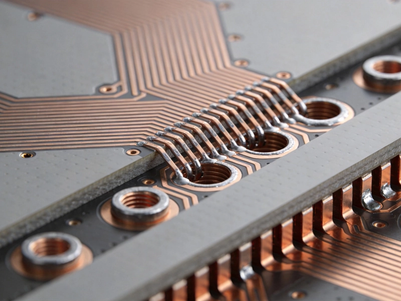
High Current PCB Thermal Vias: Array Spacing and Heat Transfer EfficiencySeptember/15/2026
Designing a High Current PCB for Industrial Welding EquipmentJuly/23/2026
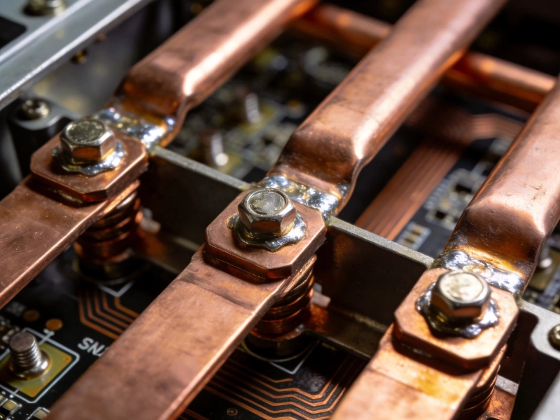
High Current PCB Design for Renewable Energy MicrogridsSeptember/30/2026
Plated Through Hole Current Rating: Complete Guide for PCB DesignersMay/21/2026
5 Critical Thermal Management Problems in High Power PCBsMay/21/2026
High Current PCB Design for Audio Amplifiers: Avoiding Ground LoopsSeptember/14/2026
High Current PCB Design for Telecommunications Base StationsSeptember/18/2026
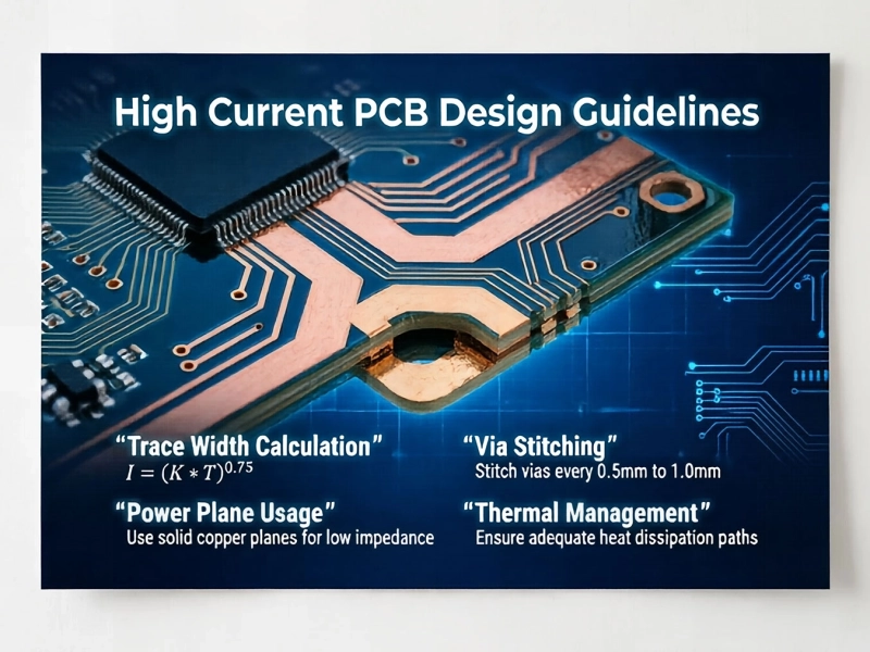
High Current PCB Design Guidelines: Ensuring Reliability and SafetyJune/08/2026