

Accurate current measurement sits at the heart of virtually every Power Electronics system. Whether you are designing a battery management system for an electric vehicle, a motor drive controller for an industrial robot, or a power supply monitoring circuit for data center equipment, the way you sense current directly impacts system efficiency, protection reliability, and overall performance. Yet choosing between the two dominant current sensing approaches and implementing them correctly on a PCB remains one of the most common sources of design errors and performance problems.
The two primary methods for measuring current in Power Electronics are shunt resistor sensing and Hall effect sensing. Each approach offers distinct advantages and faces different challenges, and the Pcb Layout requirements for each are fundamentally different. Understanding these differences and applying proper layout techniques separates designs that achieve precise, reliable current measurement from those plagued by drift, noise, and intermittent failures.
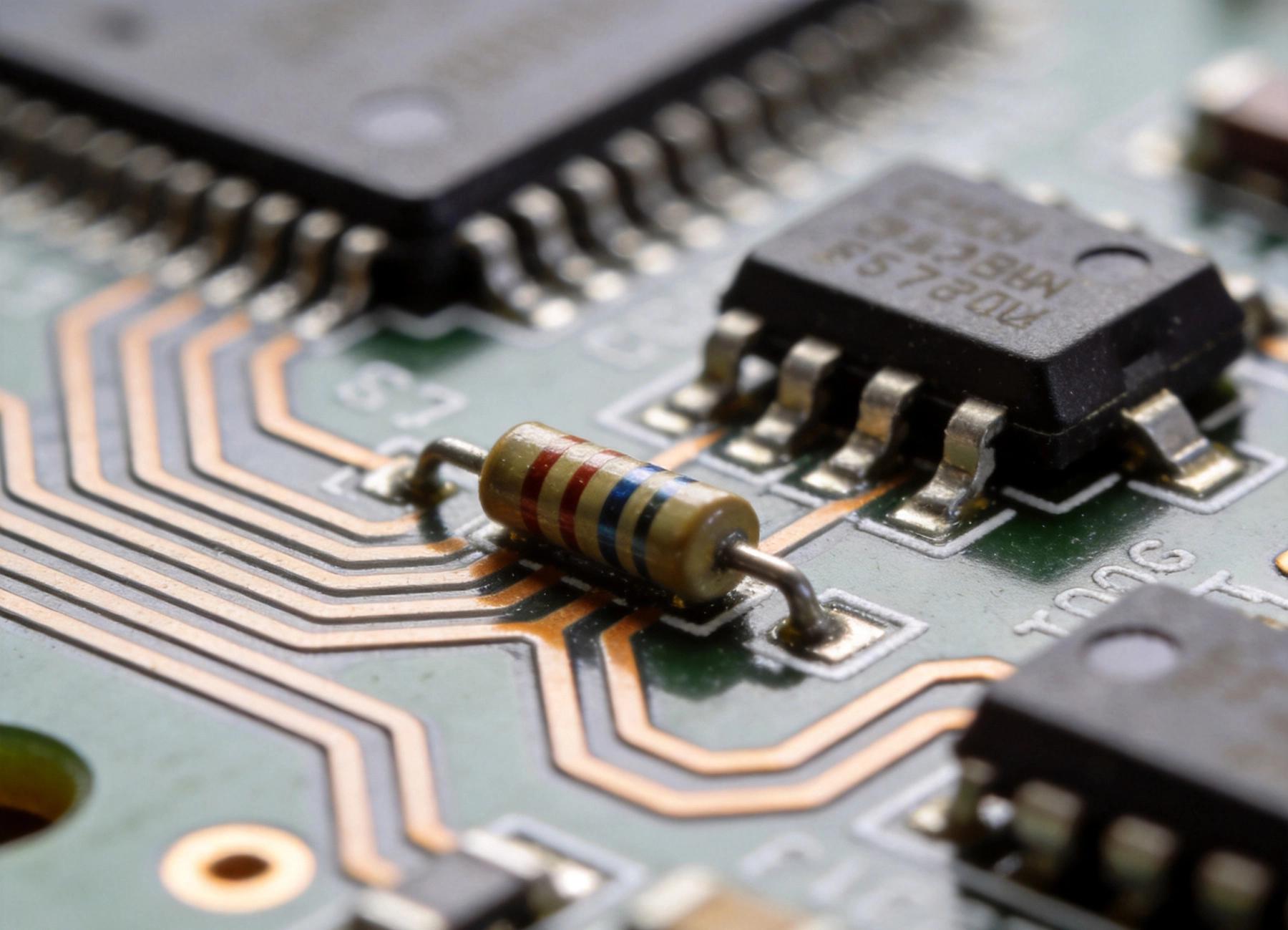
Before diving into Pcb Layout specifics, establishing a clear understanding of how each sensing method works helps explain why certain layout practices matter so much. Shunt resistor current sensing relies on Ohm's Law, placing a precision low-value resistor in series with the current path and measuring the resulting voltage drop. The relationship I = V/R means that with a known resistance, measuring voltage directly yields current. This approach is direct, predictable, and offers excellent linearity, but it introduces power loss and requires careful attention to thermal effects and parasitic resistance.
Hall effect sensing takes a fundamentally different approach, measuring the magnetic field generated around a current-carrying conductor rather than measuring voltage drop directly. When a current flows through a conductor, it produces a circular magnetic field perpendicular to the current direction. A Hall effect sensor placed in this field experiences a voltage difference proportional to the field strength, which correlates to the current magnitude. This non-contact measurement method provides inherent electrical isolation between the measurement circuit and the High Current path, but introduces sensitivity to temperature, magnetic interference, and offset drift.
Shunt resistor current sensing demands meticulous attention to PCB layout because the voltage signals involved are extremely small, often millivolts or less, while the current paths carry substantial power. The fundamental challenge is separating the tiny sense voltage from the large currents flowing through the main conductors without introducing measurement errors from parasitic resistance, thermal effects, or electromagnetic interference.
The Kelvin connection, also called four-wire sensing, represents the single most critical layout requirement for shunt resistor current sensing. This technique separates the High Current path from the voltage measurement path, ensuring that the voltage sensed across the resistor comes only from the resistor itself and not from any parasitic resistance in the Pcb Traces or solder joints.
In a properly implemented Kelvin connection, two dedicated sense traces connect directly to the inner edges of the resistor焊盘 rather than to the main current-carrying pads. These sense traces carry only the microamp-level currents required by the measurement amplifier input, allowing them to be narrow without affecting resistance. The main current pads, by contrast, must be wide and robust to handle the full measurement current with minimal resistive heating and voltage drop.
Failing to implement proper Kelvin connections introduces measurement errors that can easily reach several percent. A typical Pcb Trace contributes approximately 0.5 to 1 milliohm per square at standard Copper Weight, which means even a few squares of trace resistance in the sense path can exceed the total resistance of a 1 milliohm shunt. The temperature coefficient of copper, exceeding 3000 ppm per degree Celsius, means these parasitic resistances also drift significantly with temperature, causing measurement accuracy to degrade as the board warms during operation.
High current shunt resistors dissipate substantial power, creating Thermal Management challenges that directly affect measurement accuracy. A 100 ampere current through a 1 milliohm shunt produces 10 watts of heat, and even smaller shunts operating at tens of amperes generate significant warming. Since shunt resistor values drift with temperature, controlling thermal conditions is essential for maintaining measurement accuracy.
PCB layout should provide adequate copper area around the shunt resistor to conduct heat away from the component and into the surrounding board. Many shunt resistors come in packages with thermal pads designed for direct attachment to copper planes, and these pads should connect to large copper areas on multiple layers through Thermal Vias. The copper not only provides mechanical mounting strength but creates a thermal path that spreads Heat Dissipation across a larger area, reducing local temperature rise.
Thermal symmetry matters as much as thermal magnitude. When a shunt resistor experiences temperature gradients between its two measurement points, additional thermoelectric voltages develop that add to the measurement signal. Designing symmetric copper areas on both sides of the resistor and ensuring both sense leads connect at equivalent thermal positions minimizes this thermoelectric error source. Some precision applications go so far as to use matched Copper Trace lengths for both sense connections, ensuring identical thermal exposure.
The ground reference for the current sense amplifier requires careful consideration, particularly in systems where high currents share ground paths with sensitive measurement circuits. When substantial current flows through a ground plane, voltage drops develop along the current path, and any shared connection between power ground and measurement ground introduces these parasitic voltages into the measurement signal.
The recommended approach creates separate ground regions for the power section and the measurement section, with a single point connection between them. For low-side current sensing where the shunt connects near circuit ground, this single point should be the ground reference for the measurement amplifier, typically located at the low side of the shunt resistor. For high-side sensing where the shunt connects near the positive supply, the measurement ground must connect to the system ground at a single point that does not carry significant measurement currents.
Keep the sense trace routing short and direct, routing them as a differential pair with tight coupling to maximize common-mode rejection of any electromagnetic interference. These traces should avoid crossing over switching nodes, inductors, or other high-frequency noise sources. When routing across PCB layers is necessary, transitioning through vias positioned away from noisy switching signals maintains signal integrity.
Hall effect current sensors present a different set of PCB layout challenges centered on magnetic field management, thermal considerations, and isolation maintenance. While these sensors avoid the direct insertion loss of shunt resistors, their performance depends critically on proper placement, orientation, and environmental management.
The current-carrying conductor that generates the magnetic field detected by the Hall sensor requires careful positioning within the sensor geometry. Most integrated Hall effect current sensors feature a magnetic core or aperture that concentrates the field from the primary conductor, and proper alignment of the conductor within this structure directly affects measurement accuracy and linearity.
Sensor data sheets typically specify the acceptable position and orientation of the primary current path relative to the sensor body. Following these specifications precisely ensures the sensor operates within its calibrated measurement zone. Positioning the conductor off-center or at an angle introduces errors by changing the effective magnetic path length and the fraction of total flux coupled to the sensing element.
For sensors that require the Pcb Trace itself to serve as the primary conductor, trace width, thickness, and routing must match the sensor specifications. These requirements often specify minimum trace widths to ensure adequate Current Density and magnetic field strength, along with requirements for the number of turns when using the PCB conductor as a multi-turn primary winding. Deviations from these specifications reduce the effective sensitivity of the sensor system.
Unlike shunt resistors, Hall effect sensors respond to all magnetic fields in their environment, not just the field from the intended measurement current. This sensitivity creates vulnerability to magnetic interference from transformers, inductors, motors, and even neighboring Pcb Traces carrying substantial current. Effective layout must shield the sensor from these external field sources or position the sensor away from interference-generating components.
Physical separation represents the most reliable interference mitigation strategy. Maintaining generous spacing between the Hall sensor and inductors, transformers, or other magnetic components reduces interference proportionally to the cube of distance, making even modest increases in spacing highly effective. When spacing constraints prevent adequate separation, magnetic shielding materials such as mu-metal or soft iron cans can redirect external flux away from the sensing element.
PCB trace routing should minimize stray magnetic fields from affecting the sensor. Current loops on the PCB, whether from power delivery or signal traces, generate magnetic fields proportional to loop area. Routing high current traces as wide, closely-spaced pairs with current flowing in opposite directions minimizes net magnetic field emission. This practice, called current crowding or return path optimization, reduces the external field footprint of all PCB conductors.
Hall effect sensors exhibit sensitivity drift with temperature that requires compensation for high-accuracy applications. The Hall coefficient, which determines the relationship between magnetic field and output voltage, changes with temperature according to each sensor's specific temperature coefficient. Modern integrated sensors often include internal temperature compensation circuits, but proper PCB layout can reduce the temperature range the sensor experiences, improving overall accuracy.
Heat-generating components in the vicinity of Hall sensors create local temperature gradients that increase drift and may cause thermal equilibrium times measured in minutes after power-up. Positioning heat sources away from the sensor and providing thermal isolation through spacing or thermal barriers stabilizes the sensor temperature more quickly and reduces long-term drift.
Some Hall sensors dissipate meaningful power when processing high currents, particularly those that use internalMOSFETs for overcurrent protection or those with integrated power stages. These sensors require appropriate copper area for Heat Dissipation similar to power semiconductor devices, with thermal pad connections to multiple board layers for heat spreading.
Choosing between shunt resistor and Hall effect current sensing requires evaluating multiple system parameters against the strengths and limitations of each approach. Neither method universally outperforms the other; the correct choice depends on specific application requirements and constraints.
Shunt resistor sensing offers inherent linearity and accuracy limited primarily by resistor tolerance and stability. Precision shunt resistors with tight tolerance and low temperature coefficient can achieve measurement accuracy of 0.1% or better under controlled thermal conditions. The direct relationship between voltage and current through Ohm's Law provides a simple error model that calibration can address comprehensively.
Hall effect sensors typically achieve accuracy specifications of 0.5% to 2% for integrated devices, with higher accuracy available from more expensive precision modules. The accuracy depends on sensor calibration at specific temperature and field conditions, and drift over time and temperature adds uncertainty not present in shunt-based measurements. However, modern sensors with integrated digital interfaces often include automatic offset and sensitivity calibration that approaches shunt resistor accuracy in many applications.
Hall effect sensors provide inherent galvanic isolation between the primary current path and the measurement output, a critical advantage in high-voltage systems where connecting measurement circuitry directly to high voltage would be dangerous or impractical. Isolation ratings of 2.5 kV to 5 kV are common, enabling use in motor drives, solar inverters, and other systems operating at hundreds of volts.
Shunt resistor sensing provides no isolation; the measurement circuit must share a common reference with the measured current path. For high-side current measurement in high-voltage systems, this requires measurement amplifiers with high common-mode voltage capability or isolated amplifier circuits that add complexity and cost. When isolation is required, adding an isolation barrier between the shunt measurement and the system processor adds cost and potentially compromises bandwidth.
Shunt resistors continuously dissipate power proportional to the square of measured current, creating efficiency loss that can become significant in high-current applications. A 1 milliohm shunt carrying 100 amperes dissipates 10 watts continuously, representing a meaningful efficiency penalty in battery-powered or high-efficiency power conversion systems. Reducing shunt resistance to lower power loss unfortunately reduces the measurement signal, challenging the signal-to-noise ratio of the measurement.
Hall effect sensors dissipate minimal power in the primary current path since they do not insert resistance. Some sensors have internal power dissipation from signal conditioning and output circuitry, but this is typically milliwatts rather than watts. For applications where efficiency is paramount or where heat management is difficult, this zero insertion loss represents a substantial advantage.
Shunt resistor current sensing offers essentially unlimited bandwidth, limited only by the amplifier and measurement circuitry. Measurement bandwidths of 1 MHz or more are achievable with appropriate op-amp selection, making shunt sensing suitable for fast transient detection, overcurrent protection in switching converters, and control loop feedback in high-frequency power supplies.
Hall effect sensors operate through magnetic field coupling that introduces delays from eddy currents in magnetic materials and the limited speed of the Hall element itself. Typical bandwidths range from 20 kHz for open-loop sensors to 100 kHz or more for closed-loop designs. While adequate for most motor control and power supply monitoring applications, this limited bandwidth may exclude Hall sensing from the fastest Switching Converter applications.
Different application categories tend to favor different sensing approaches based on the relative importance of various performance parameters. Understanding these typical preferences helps narrow the selection process for new designs.
Battery management systems in electric vehicles, energy storage systems, and portable electronics typically favor shunt resistor sensing for charge and discharge current monitoring. The high accuracy requirement, moderate current levels, and need for precise state-of-charge estimation align well with shunt resistor capabilities. Isolation requirements are usually manageable since battery voltages typically remain within range accessible to non-isolated amplifiers, and the cost efficiency of shunt sensing provides advantage in the cost-sensitive consumer and automotive markets.
Motor drive applications frequently employ Hall effect sensors for overcurrent protection and current loop feedback in three-phase inverter systems. The high common-mode voltages present on motor phases make isolated sensing essential, and Hall sensors provide this isolation without external isolation components. Motor drives also often require modest bandwidth compared to switching converters, fitting within Hall sensor capabilities while benefiting from the isolation and simplified high-side current measurement.
High-efficiency power supplies and DC-DC converters present mixed requirements that often favor shunt resistor sensing for output current measurement. The efficiency emphasis makes insertion loss unacceptable, while the need for fast transient response during load changes demands high measurement bandwidth. shunt sensing in the low-side position or with appropriate high-side amplifiers addresses these requirements, though isolation may need to be added if the converter topology creates high common-mode voltage challenges.
Proper verification testing confirms that the current sensing implementation achieves the required performance. Testing should validate both static accuracy under controlled conditions and dynamic performance under actual operating conditions.
Static accuracy testing measures the current sensing output across the expected measurement range at controlled temperature and compares against a reference measurement standard. At each test current level, record the difference between the sensed value and the reference to calculate accuracy. Temperature testing repeats this characterization across the expected operating temperature range to verify drift specifications.
Dynamic testing applies step changes in current or pulsed loads to observe measurement response. The recorded waveform should show clean, monotonic response without oscillation or excessive overshoot. Observing the measurement under actual switching conditions with oscilloscope probes on the sense nodes reveals any susceptibility to electromagnetic interference from the power stage switching transients.
High Current Pcb current sensing demands attention to fundamentally different design priorities depending on whether shunt resistor or Hall effect sensing is selected. Shunt resistor layouts must focus on Kelvin connections, Thermal Management, and ground plane integrity to achieve accurate measurements of tiny voltage signals in the presence of large currents. Hall effect layouts must manage magnetic field integrity, minimize thermal gradients, and position the sensor to avoid interference from external fields.
Neither approach universally outperforms the other. Shunt sensing excels in applications requiring highest accuracy, widest bandwidth, and cost-effective implementation in systems with manageable common-mode voltage. Hall sensing provides inherent isolation, zero insertion loss, and simplified high-side current measurement for high-voltage systems. Matching the sensing approach to application requirements and implementing proper layout for the chosen method determines whether a design achieves the current measurement performance that the system needs.
Thorough verification testing under realistic operating conditions catches layout-related issues before they reach production. Current sensing problems discovered during system integration or field deployment are among the most difficult to diagnose and resolve, making investment in proper initial design and verification testing consistently worthwhile.

Designing a High Current PCB for Industrial Welding EquipmentJuly/23/2026
Designing a High Current PCB Motor Driver: Avoiding EMI PitfallsJuly/14/2026
Designing a 100A High Current PCB for EV Battery Management SystemsJuly/09/2026
High Current PCB Design GuidelinesMay/21/2026
Mastering IPC-2152 Current Carrying Capacity Calculation for Reliable PCB DesignJune/04/2026

High Current PCB Design Guidelines: Ensuring Reliability and SafetyJune/08/2026

5 Critical Thermal Management Problems in High Power PCBsMay/21/2026
Plated Through Hole Current Rating: Complete Guide for PCB DesignersMay/21/2026